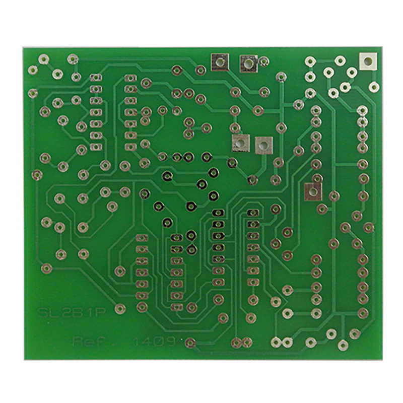
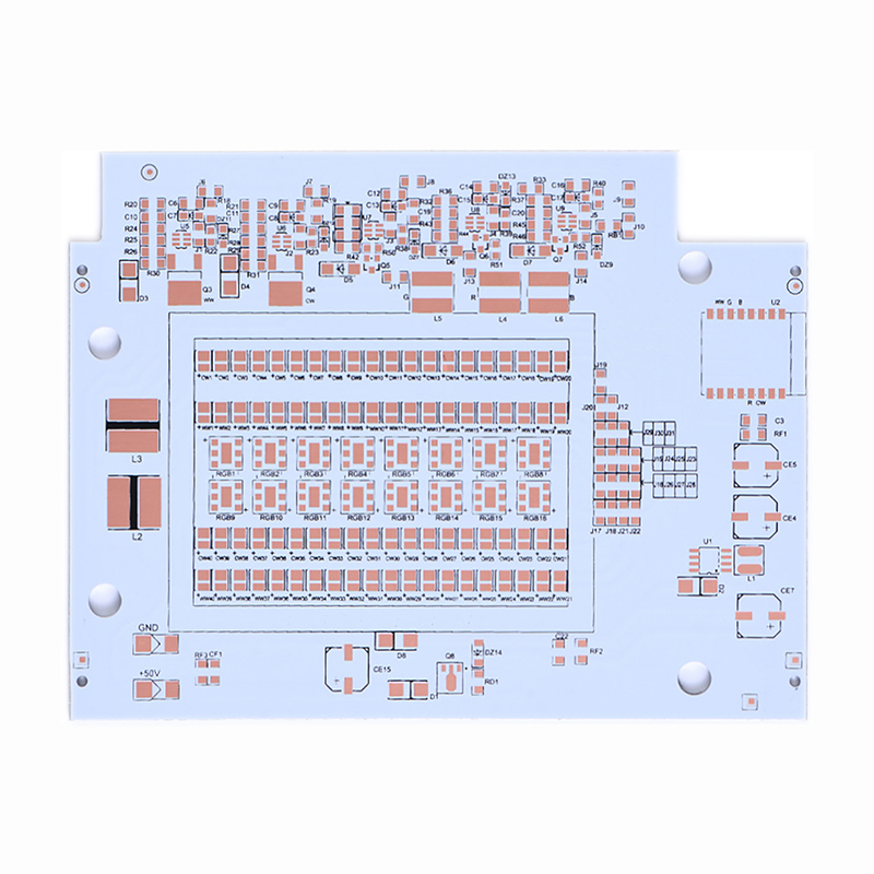
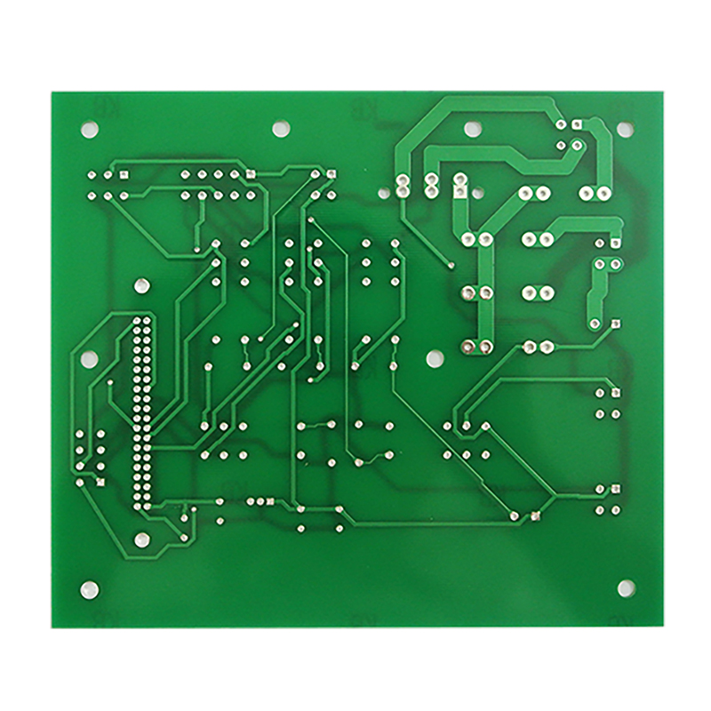
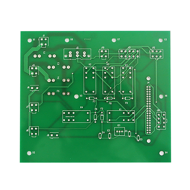
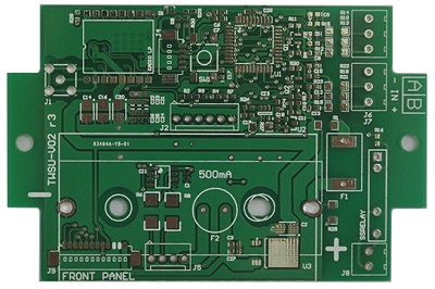
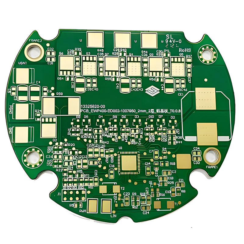
 PCB
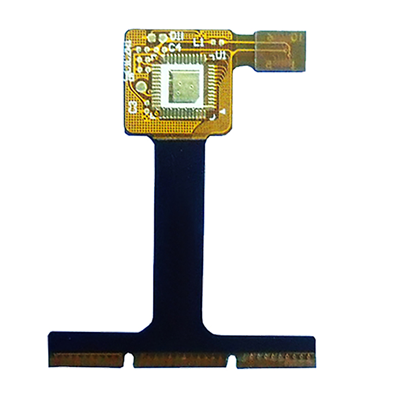
PCB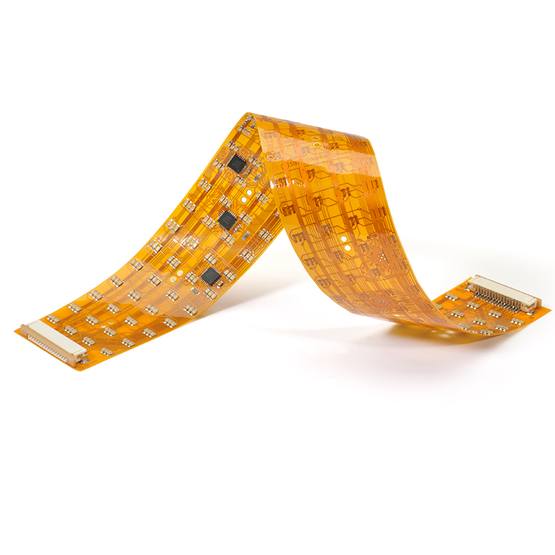 FPC
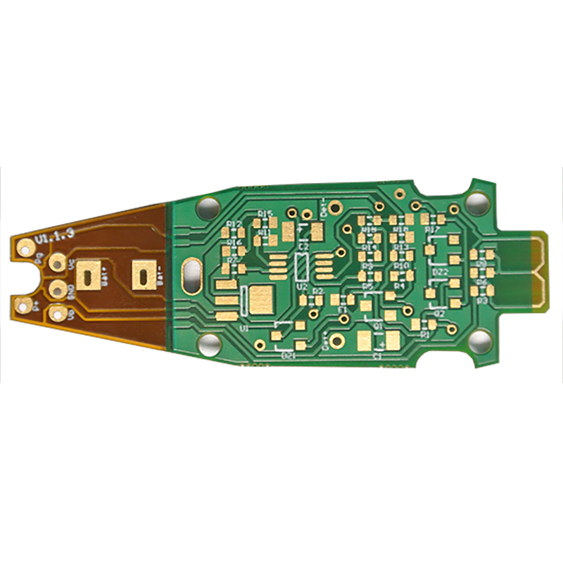
FPC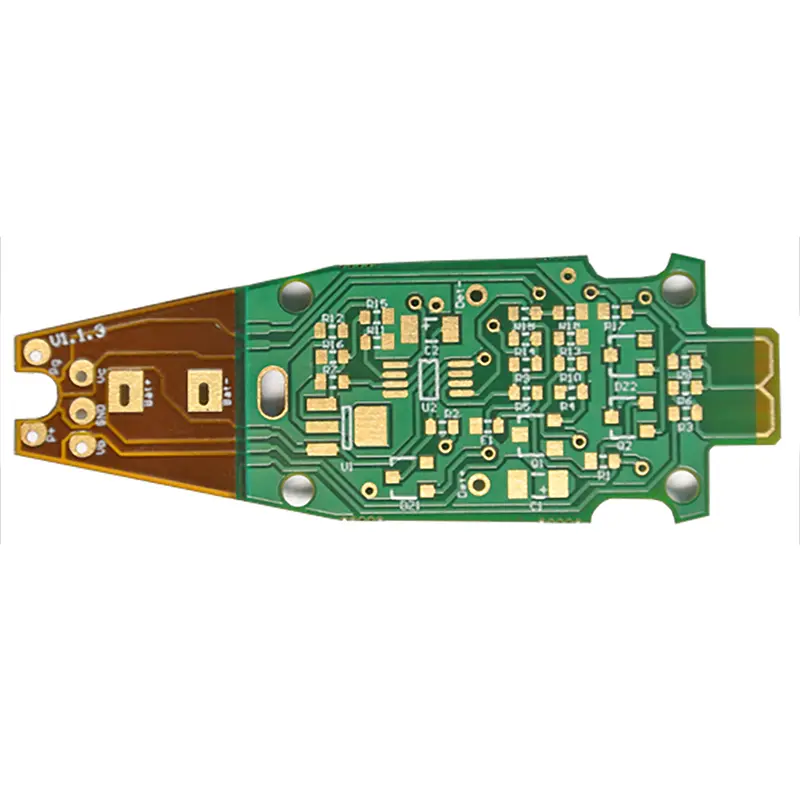 Rigid-Flex
 FR-4
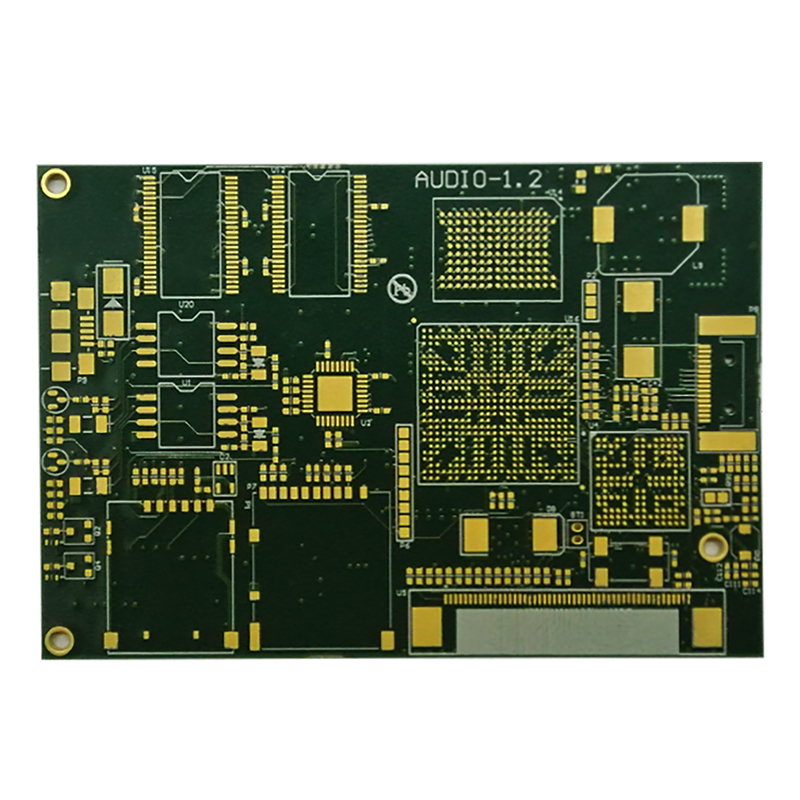
FR-4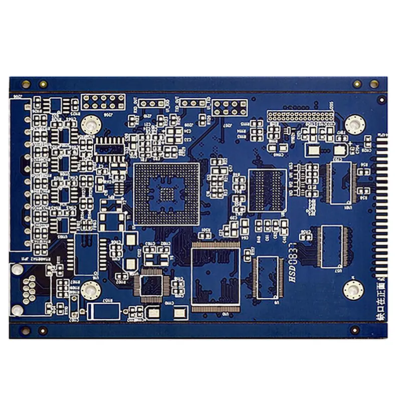 HDI PCB
 Aluminum
 Copper Core
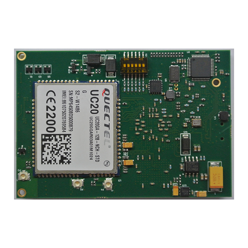
 PCB Assembly
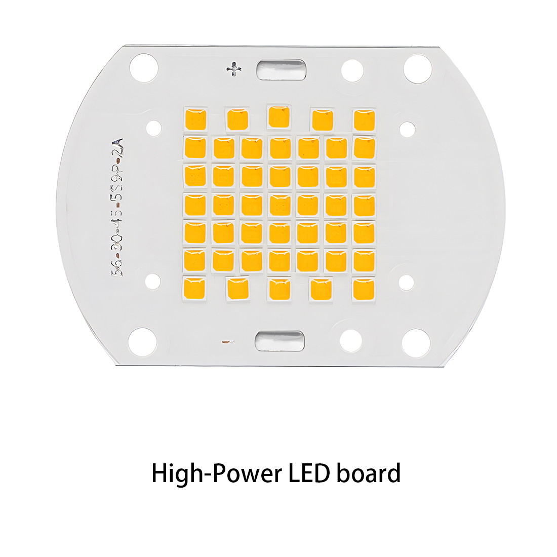 LED light PCBA
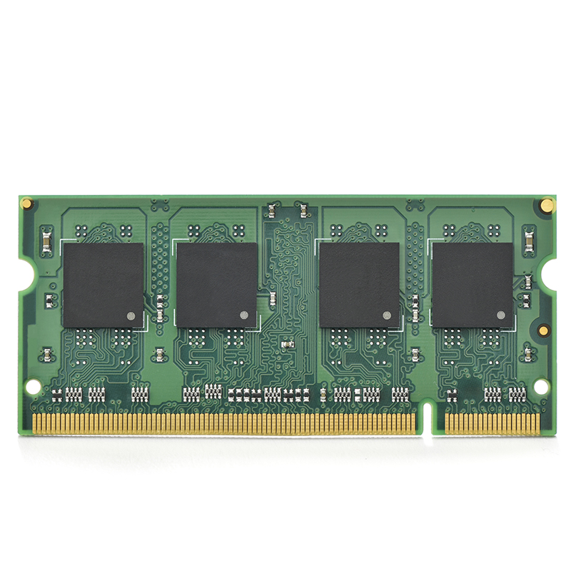
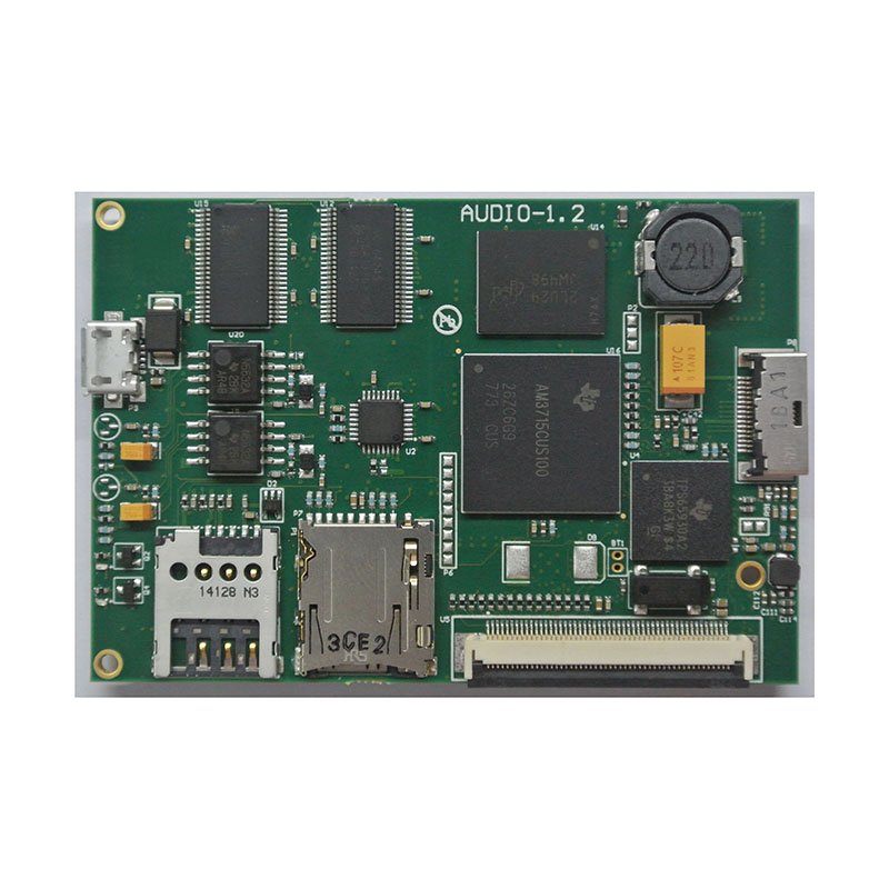
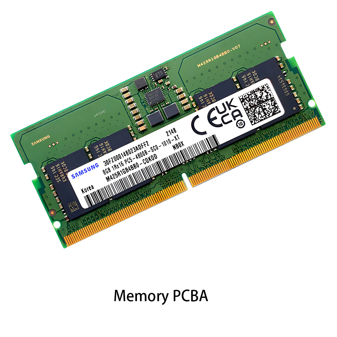 Memory PCBA
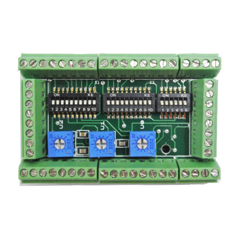
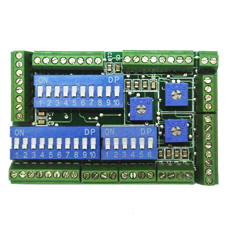
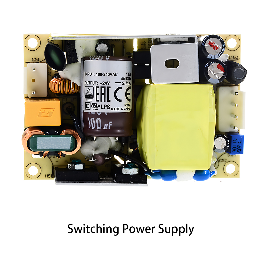 Power Supply PCBA
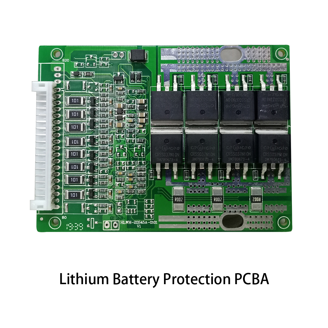 New Energey PCBA
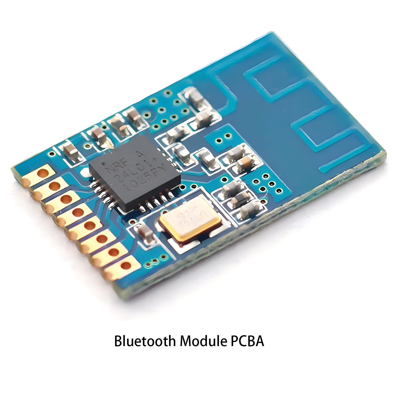 Communication PCBA
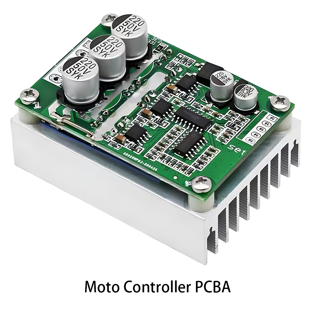 Industrial Control PCBA
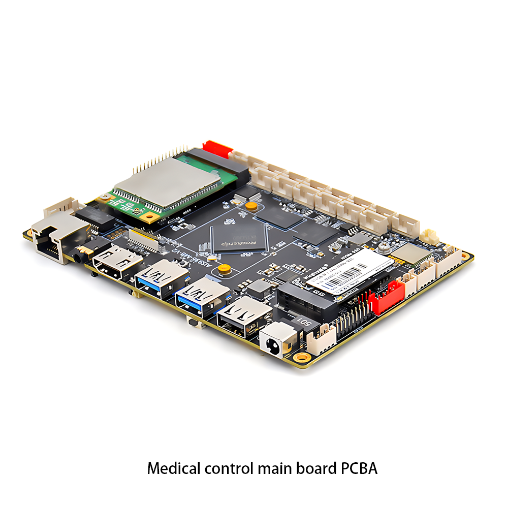 Medical Equipment PCBA
 Product Rebuild
 PCB Copy
 IC Cracking
 Testing Service
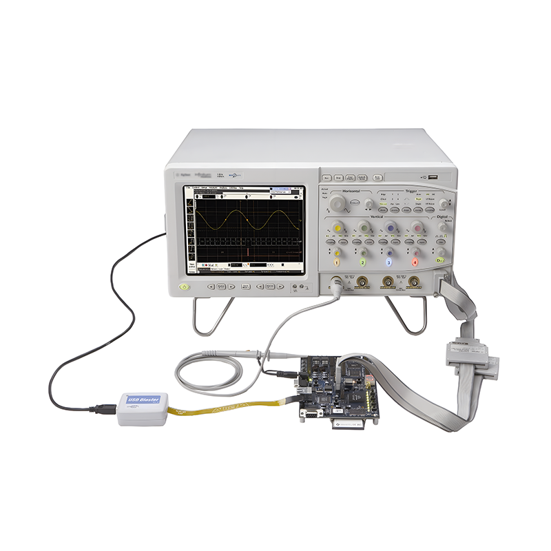 PCBA Testing Service
 Certification Application
 RoHS Certification Application
 REACH Certification Application
 CE Certification Application
 FCC Certification Application
 CQC Certification Application
 UL Certification Application
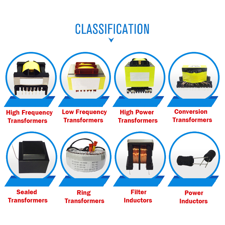
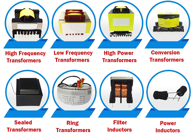 Transformers, Inductors
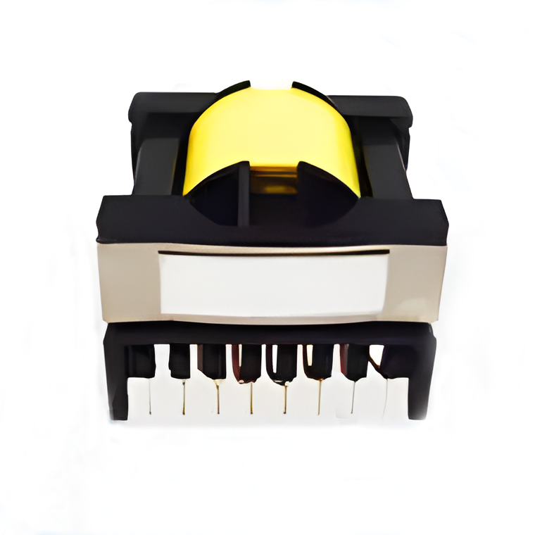 High Frequency Transformers
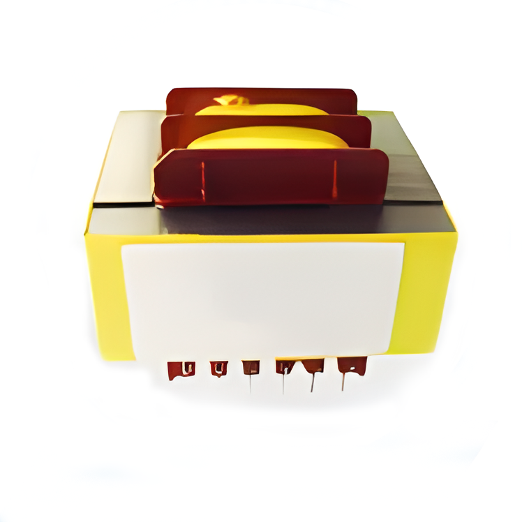 Low Frequency Transformers
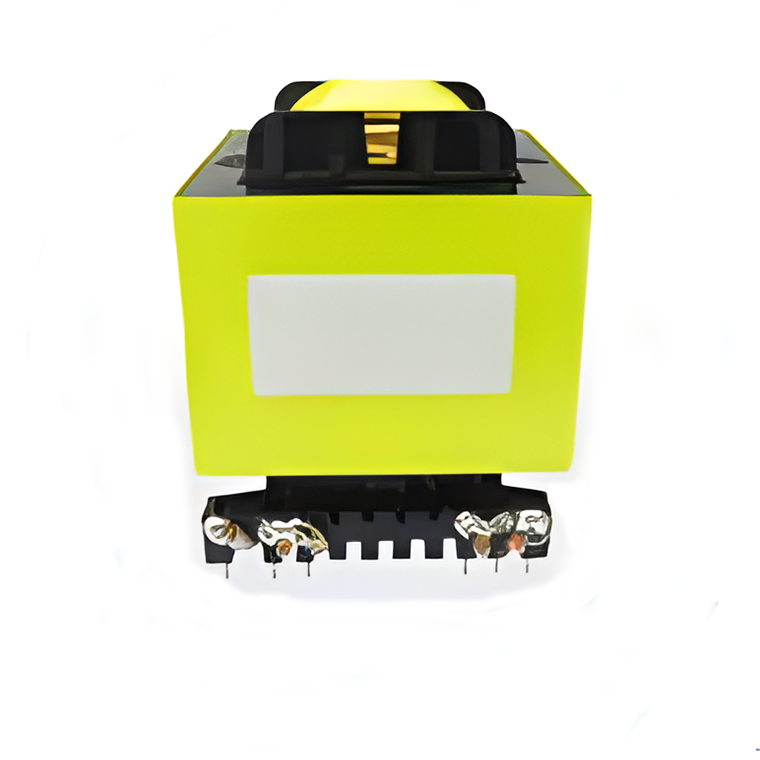 High Power Transformers
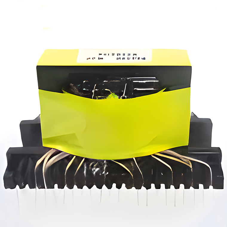 Conversion Transformers
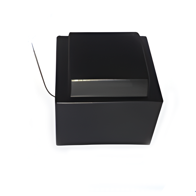 Sealed Transformers
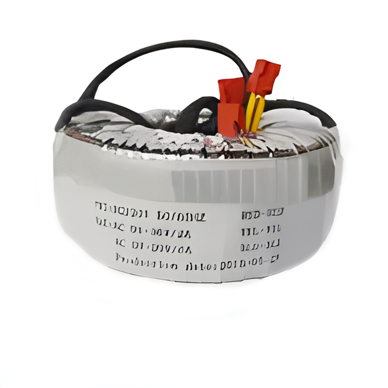 Ring Transformers
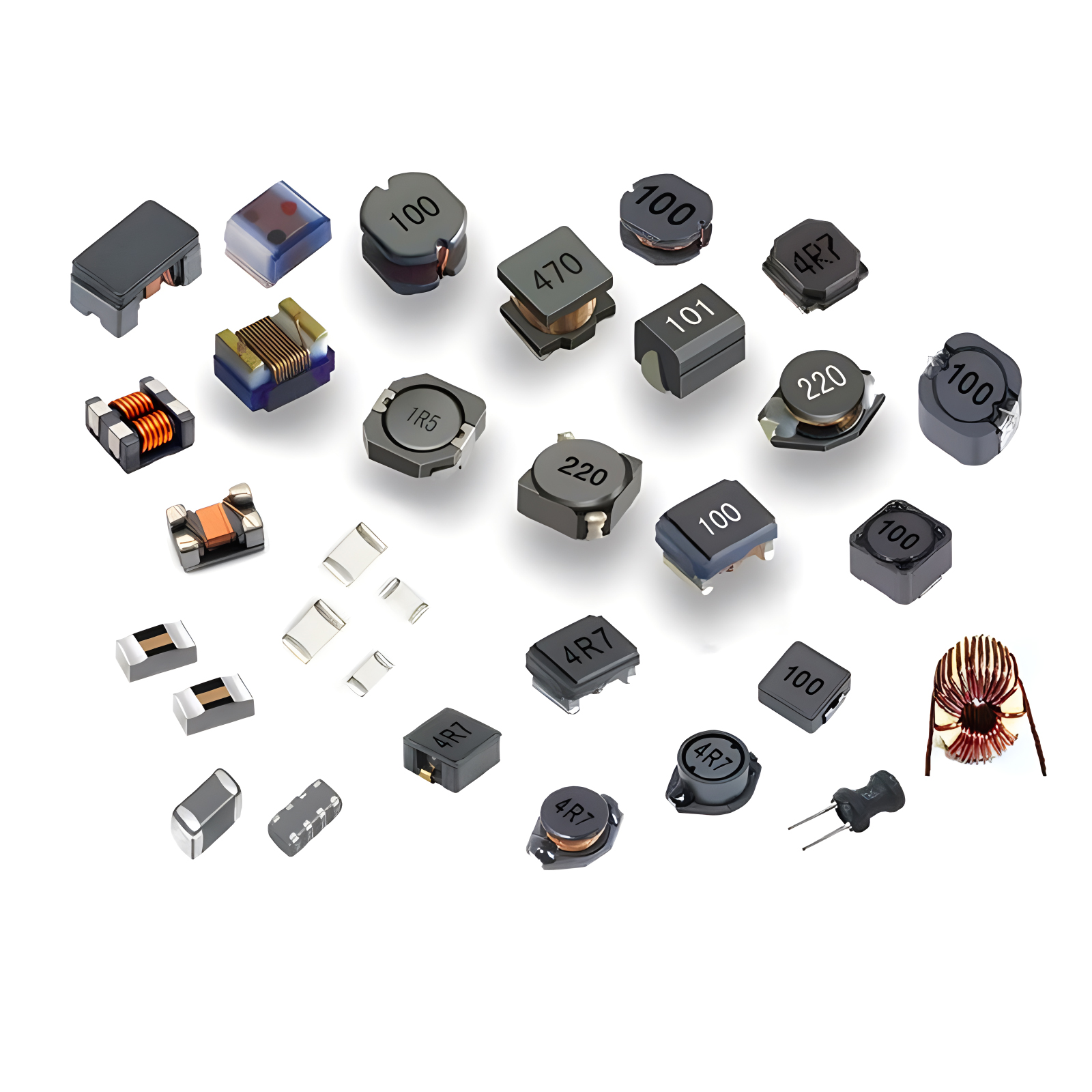 Inductors
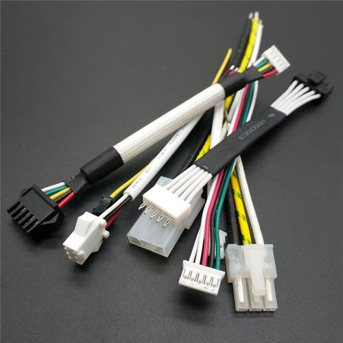
 Wires,Cables Customized
 Network Cables
 Power Cords
 Antenna Cables
 Coaxial Cables
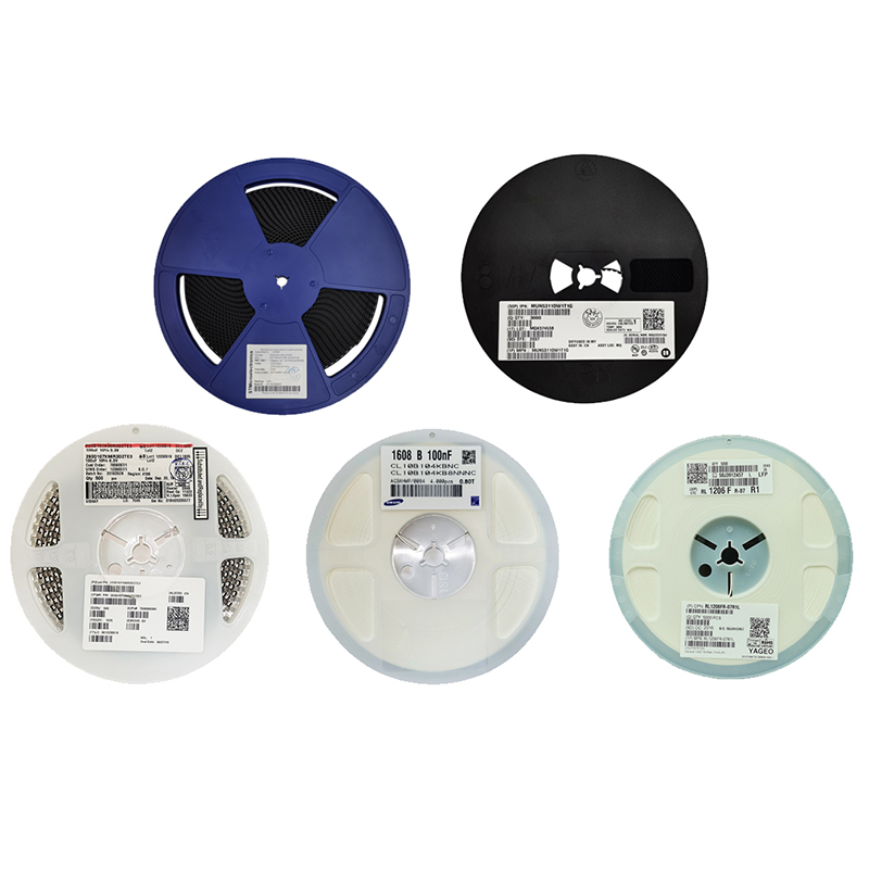
 Capacitors
 Connectors
 Diodes
 Schottky Barrier Diodes
 General Purpose Diodes
 Switching Diodes
 Bridge Rectifiers


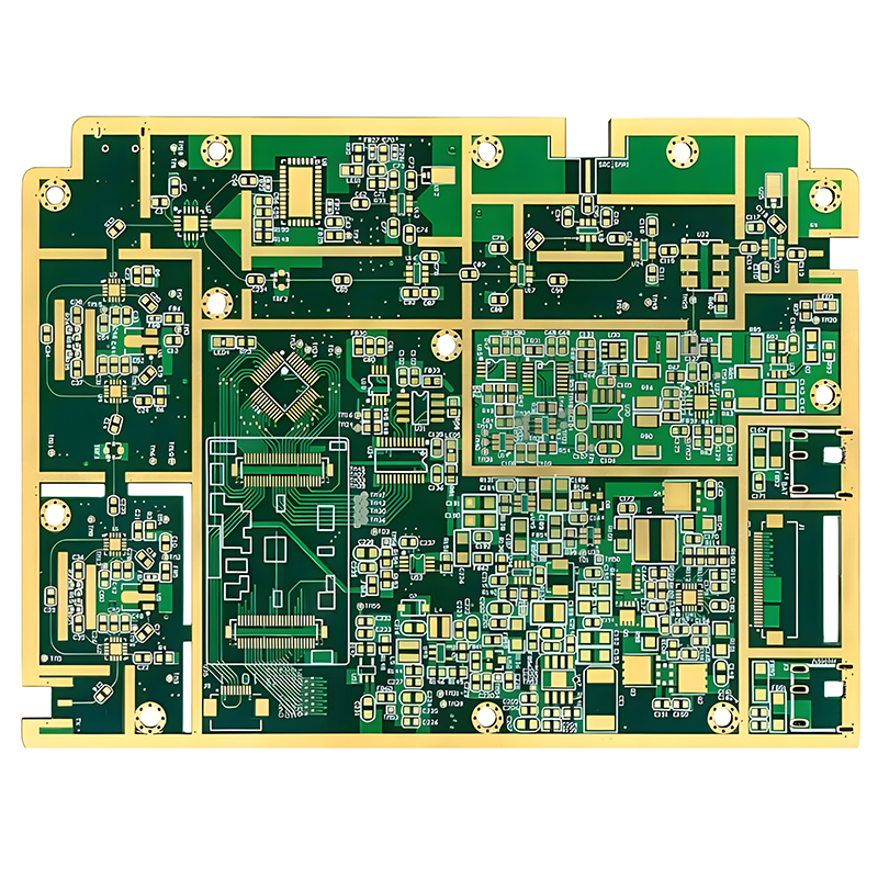
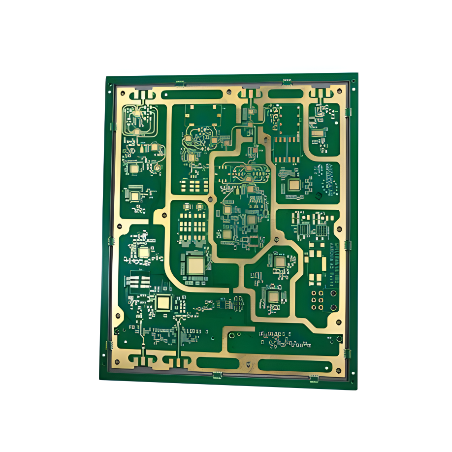
HDI PCB
By utilizing advanced production technology and strict quality control system, we ensure that every piece of HDI PCB meets the actual needs of customers. We always adhere to the customer-oriented principle and provide the best service to customers.
| HDI (Partial Technology Capability) | |
| N/M/N | 4~28L(6 Steps) |
| Interconnection of any layer | 16L |
| Finished board thickness | 200um~3200um |
| Copper Foil Type | VLP. SLP. SLP2 |
| Min laser via/pad(um) | 70/140um |
| Min buried via diameter/pad(um) | 100/230um |
| Min PTH diameter/pad(um) | 100/230um |
| Min trace/spacing(um) | 35/35um |
| Min solder mask openging(um) | 90um |
| Solder mask color |  |
| Surface Finish |
HASL/ImmersionTin/ImmersionSilver /ImmersionGold/ENEPIG/OSP |
| Test | ICT, FCT, AOI, Flying probe test |
For more information, please click 【here】.


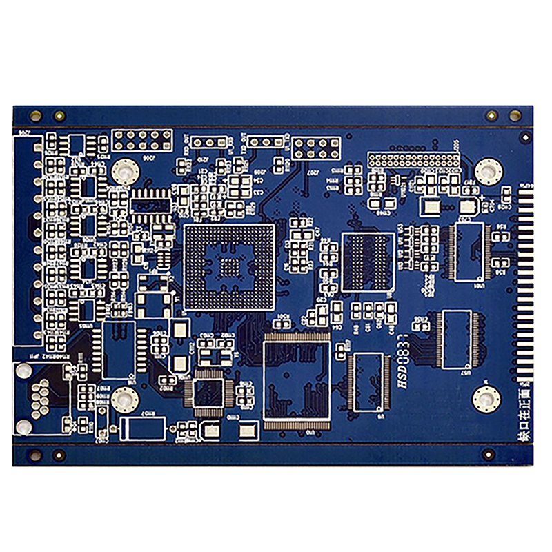
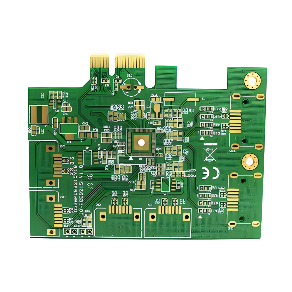
FR-4|Advanced PCB
PCB sampling and mass production services from 1 to 42 layers. We use real A-grade plates, adhere to the factory's self-operated production model, and ensure the reliability and stability of quality. Brand new high-rise dedicated production line, the circuit soldering prevention adopts advanced production equipment in the industry such as LDI, VCP pulse plating, etc., uses famous brand plates, precise impedance detection instruments, and provides high-definition characters, high-quality inspection standards, high-end packaging and transportation services.
| Multi-Layers(Partial Technology Capability) | ||
| Layer count | 1~42L | |
| Core thickness(Exclude copper) | 50um | |
| Min mechanical hole size | 100um | |
| Inner outter layer registration Mini pad Dia. | DHS+6mil | |
| Min. S/M dam | 50um | |
| Min. S/M opening size | 4mil | |
| Via Covering | Epoxy Filled & Untented, Epoxy Filled & Capped,Copper paste Filled & Capped | |
| Solder mask color |  |
|
| Solder mask ink thickness | ≧10um | |
| Depth-Controlled routing tolerance | ±0.05mm | |
| Minimum Legend Width | 6mil(0.15mm) | |
| Surface Finish |
HASL/ImmersionTin/ImmersionSilver /ImmersionGold/ENEPIG/OSP |
|
For more information, please click 【here】.
PTFE Teflon high-frequency board
| Partial PCB Process Parameters | |
| Base Material | PTFE Teflon |
| Layers | 2Layers |
| Maximum Dimensions | 590mm*438mm |
| PCB Thickness | 0.76mm~1.65mm |
| PCB Color | |
| Silkscreen |  |
| Material Type |
ZYF255DA(Dk=2.55,Df=0.0018), ZYF265D(Dk=2.65,Df=0.0019), ZYF300CA-C(Dk=2.94,Df=0.0016), ZYF300CA-P(Dk=3.0,Df=0.0018), [Data Sheet] |
| Surface Finish | ENIG |
| Gold Thickness | 1μ'', 2μ'' |
| Outer Copper Weight | 1oz |
| Via Covering | Tented, Untented, Plugged, Epoxy Filled & Capped, Copper Paste Filled & Capped |
| Test | AOI, Flying Probe Test |
Rogers high-frequency board
| Partial PCB Process Parameters | |
| Base Material | Rogers |
| Maximum Dimensions | 590mm*438mm |
| Layers | 1Layer, 2Layers |
| PCB Thickness | 0.5mm~1.6mm |
| PCB Color | |
| Silkscreen | |
| Material Type | RO4350B(Dk=3.48,Df=0.0037) [Data Sheet] |
| Surface Finish | ENIG |
| Gold Thickness | 1μ'', 2μ'' |
| Outer Copper Weight | 1oz |
| Via Covering | Tented, Untented, Plugged, Epoxy Filled & Capped, Copper Paste Filled & Capped |
| Test | AOI, Flying Probe Test |