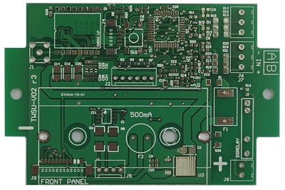
 PCB
PCB FPC
FPC Rigid-Flex
 FR-4
FR-4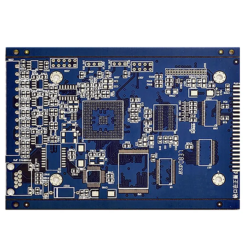 HDI PCB
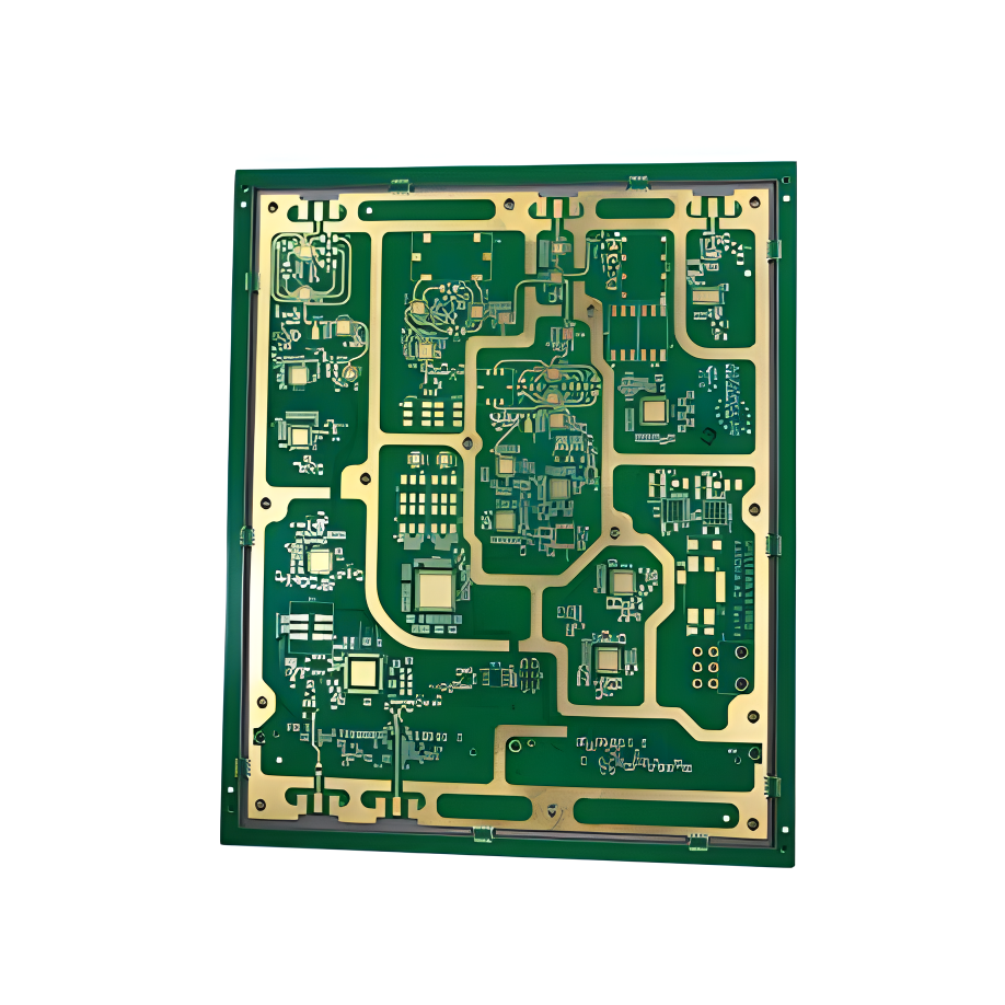 Rogers High-Frequency Board
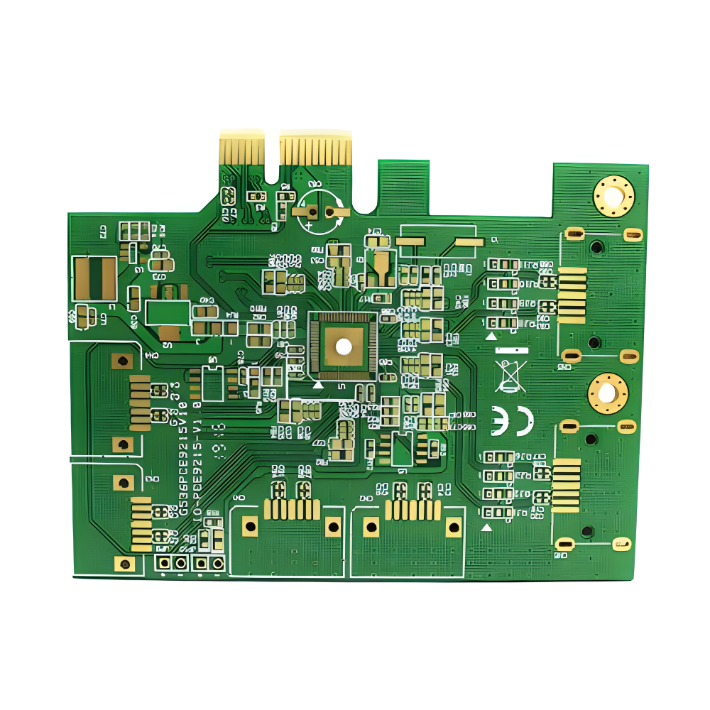 PTFE Teflon High-Frequency Board
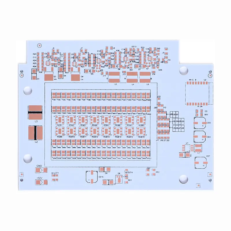 Aluminum
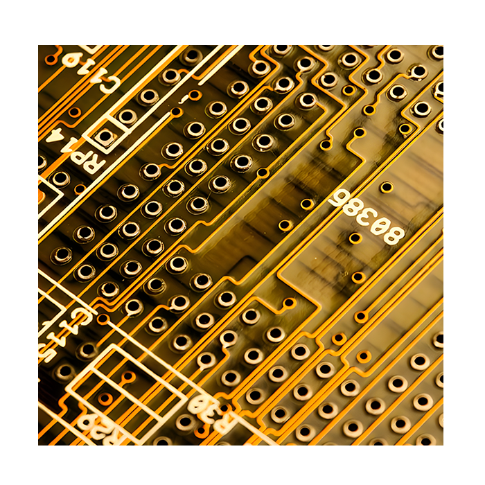 Copper Core
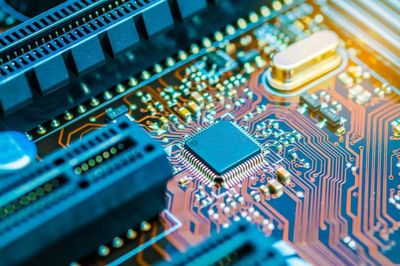 PCB Assembly
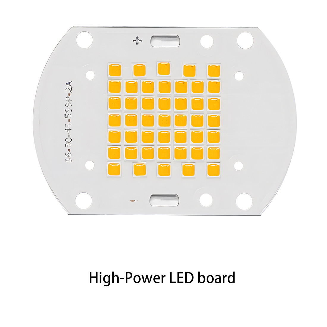 LED light PCBA
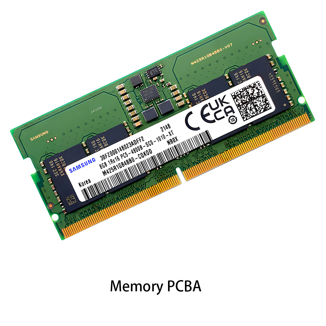 Memory PCBA
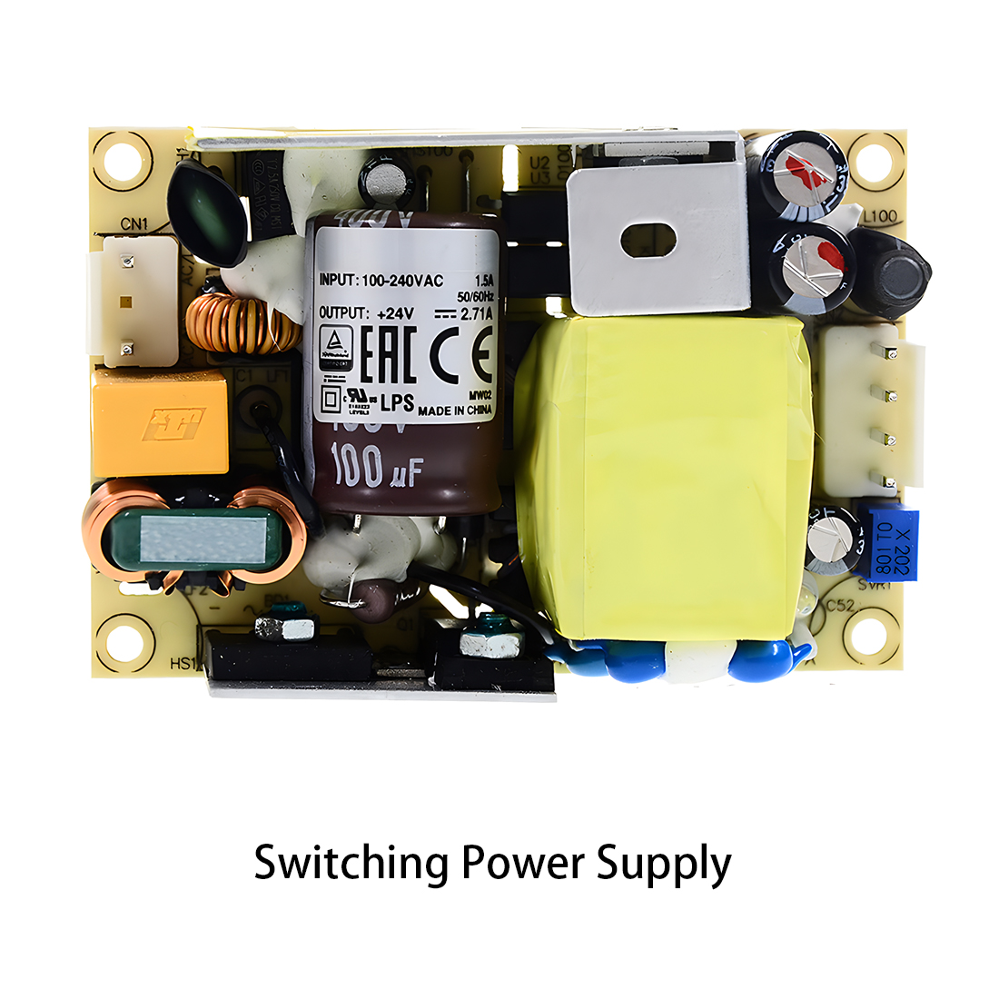 Power Supply PCBA
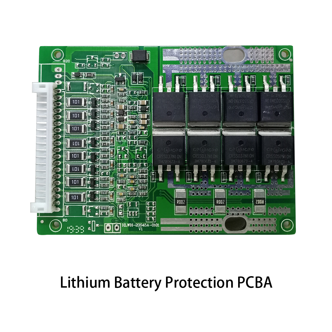 New Energey PCBA
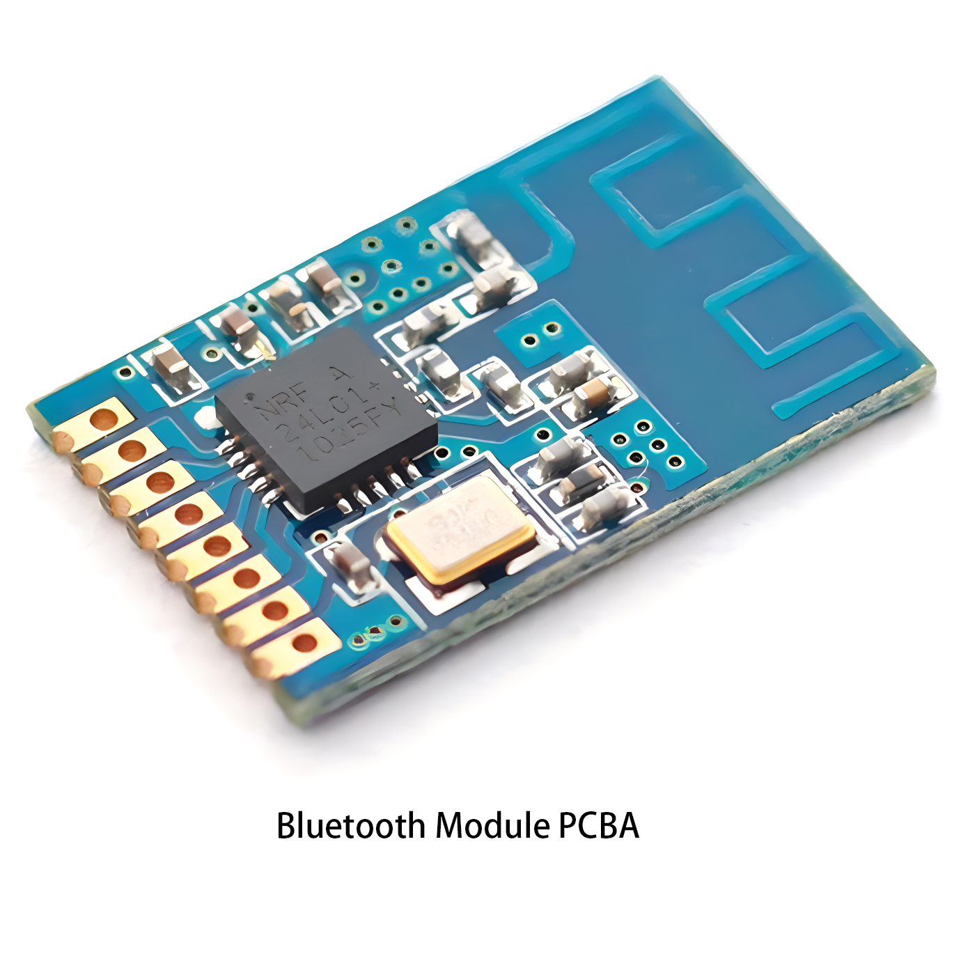 Communication PCBA
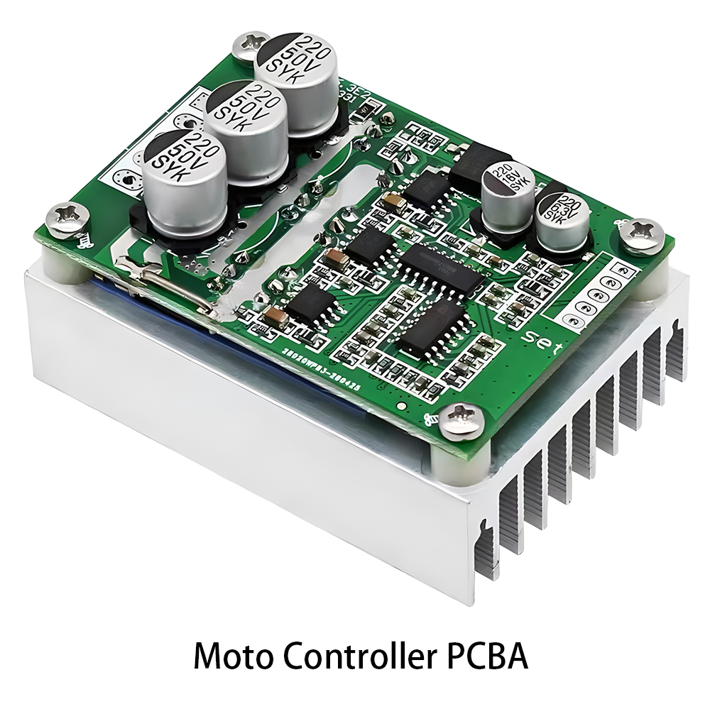 Industrial Control PCBA
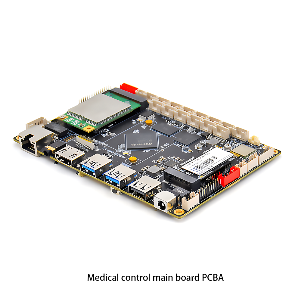 Medical Equipment PCBA
 Product Rebuild
 IC Cracking
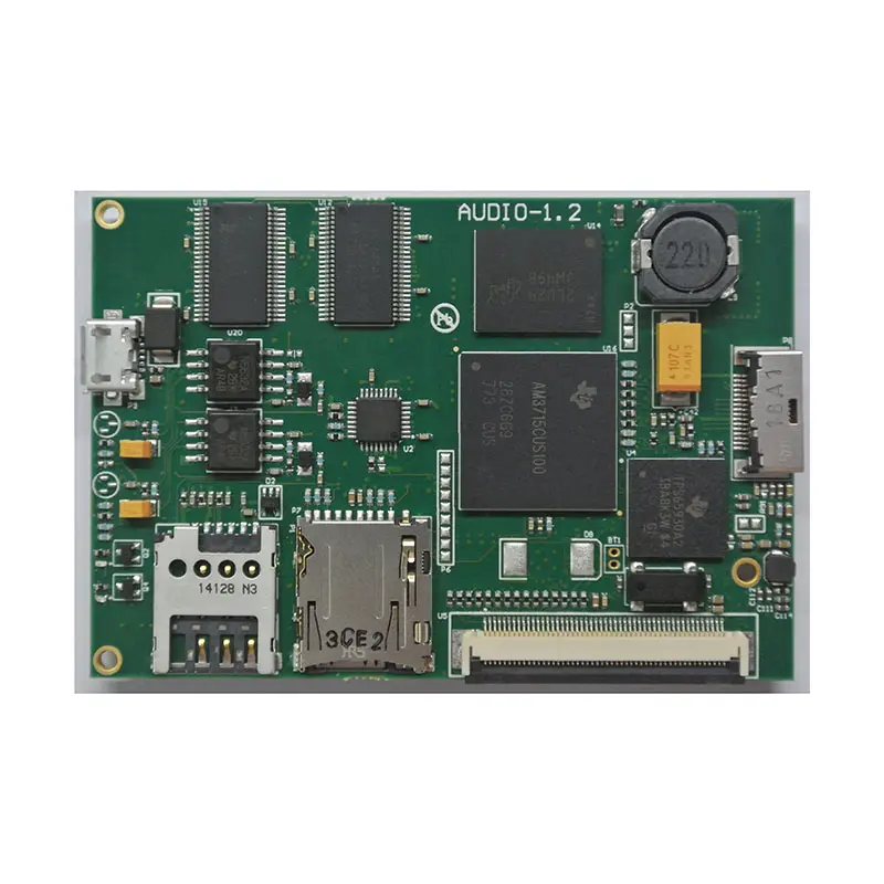 Testing Service
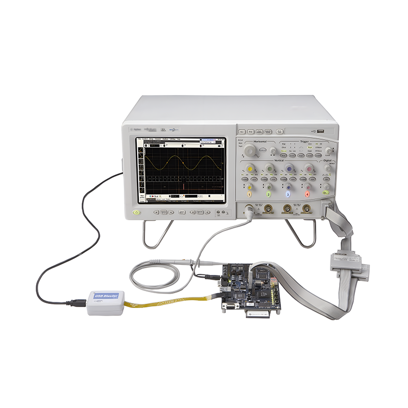 PCBA Testing Service
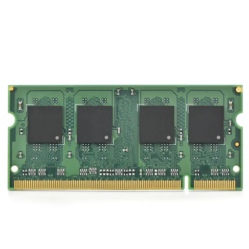 Certification Application
 RoHS Certification Application
 REACH Certification Application
 CE Certification Application
 FCC Certification Application
 CQC Certification Application
 UL Certification Application
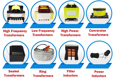 Transformers, Inductors
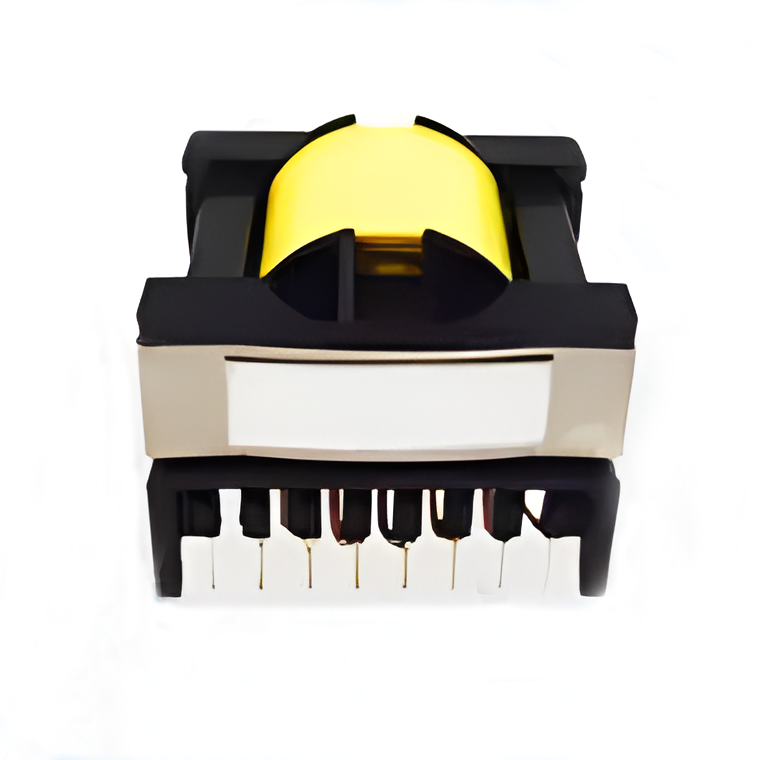 High Frequency Transformers
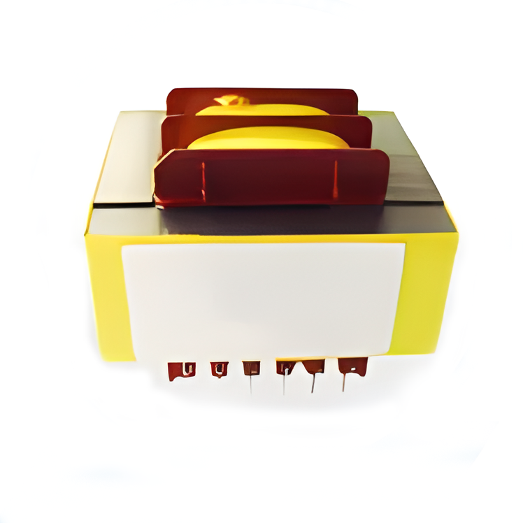 Low Frequency Transformers
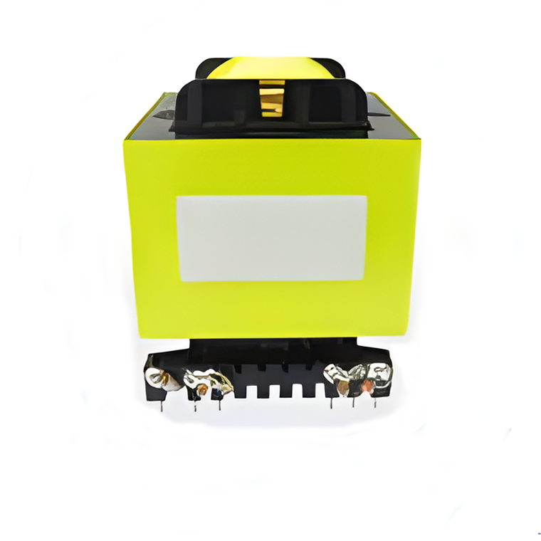 High Power Transformers
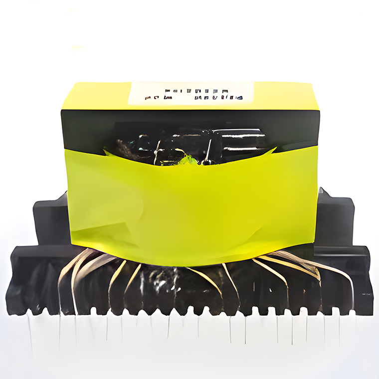 Conversion Transformers
 Sealed Transformers
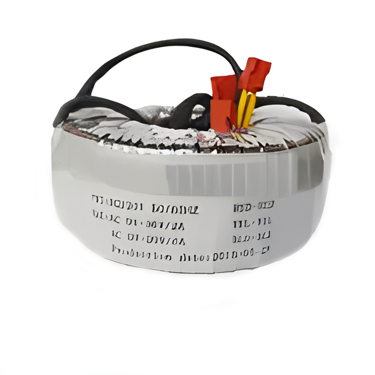 Ring Transformers
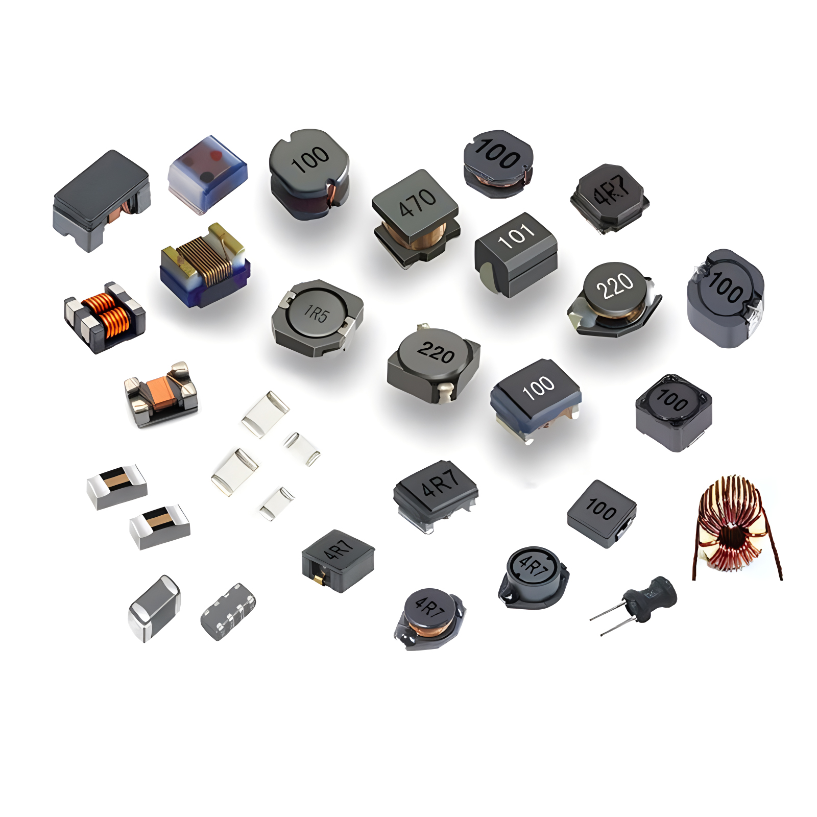 Inductors
 Wires,Cables Customized
 Network Cables
 Power Cords
 Antenna Cables
 Coaxial Cables
 Capacitors
 Connectors
 Diodes
 Schottky Barrier Diodes
 General Purpose Diodes
 Switching Diodes
 Bridge Rectifiers


PCB Copy
Detailed Process of Copying a PCB Board without Components
I. Preparation Phase
1、Inspect the PCB Board: Ensure the PCB board is free of components and the surface is clean, with no residual dirt or contaminants.
2、Prepare Tools: Gather necessary tools such as a scanner, alcohol, water sandpaper, a laser printer, transparent film, and PCB copying software (e.g., PROTEL, Quickpcb2005, etc.).
II.Scanning and Image Processing
1、Scan the PCB Board:
* Place the PCB board in a scanner, ensuring it's level and straight for accurate scanning.
* Adjust the scanner's pixel settings for a clear scan result. Higher pixel settings generally capture more detail.
2、Process the Image:
* Open the scanned image in an image processing software (e.g., PHOTOSHOP).
* Adjust contrast and brightness to create a strong contrast between copper traces and non-copper areas.
* Convert the image to black and white, and check for clear line visibility. If not clear, repeat contrast and brightness adjustments.
* Save the processed image as a BMP file, typically named TOP.BMP (top layer) and BOT.BMP (bottom layer).
III. Conversion and Drawing
1、Convert File Format:
* Use PCB copying software to convert the BMP files into a format recognizable by PROTEL or other EDA software.
* Open the converted files in PROTEL or the EDA software, checking for alignment of PADs and VIAs (vias). Adjust if necessary by returning to image processing.
2、Draw the PCB Layout:
* In PROTEL or the EDA software, draw the PCB's top and bottom layers based on the scanned images and converted files.
* Place devices on the SILK layer (usually yellow) and adjust according to actual dimensions and layout requirements.
* After drawing, delete the SILK layer and verify all layers are complete.
IV. Verification and Output
1、Verify the PCB Layout:
* Print the drawn PCB layout onto transparent film using a laser printer at a 1:1 scale.
* Overlay the film on the original PCB board for comparison, ensuring all lines and layouts match.
2、Output PCB Files:
* If verification is successful, export the PCB files in a format acceptable to the manufacturing factory (e.g., Gerber files).
* Send the exported files to the PCB manufacturing factory for production.
V. Notes
* Handling Multi-layer Boards: For multi-layer PCBs, repeat scanning, image processing, and drawing for each layer. Inner layers may require chemical etching or sandpaper grinding for layer separation.
* Precision and Patience: PCB copying requires high precision and patience. Even minor deviations can affect the quality and fit of the copied board.
* Testing and Debugging: After manufacturing, test and debug the PCB to ensure its electronic performance matches the original.
This process outlines the steps for copying a PCB board without components, emphasizing the importance of precision, patience, and thorough verification at each stage.