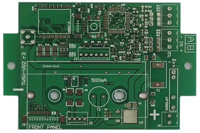
 PCB
PCB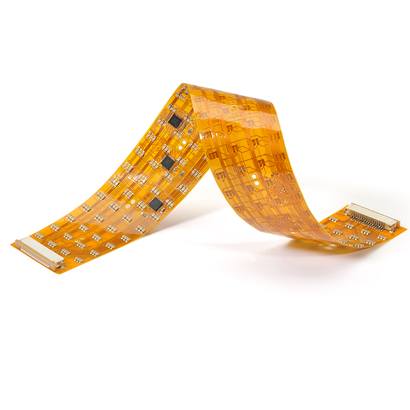 FPC
FPC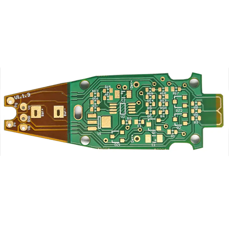 Rigid-Flex
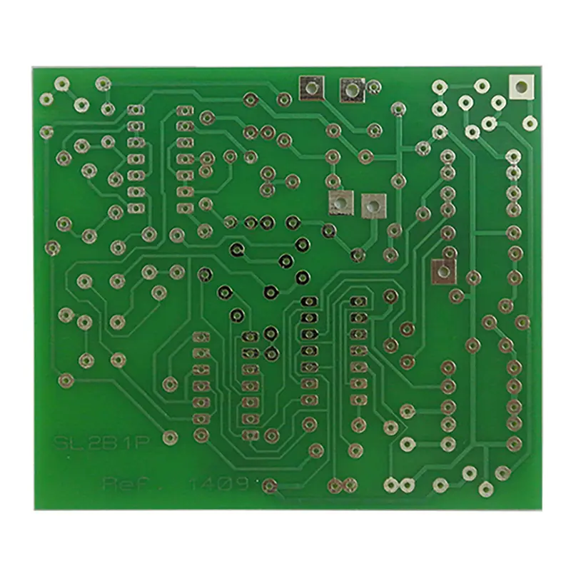 FR-4
FR-4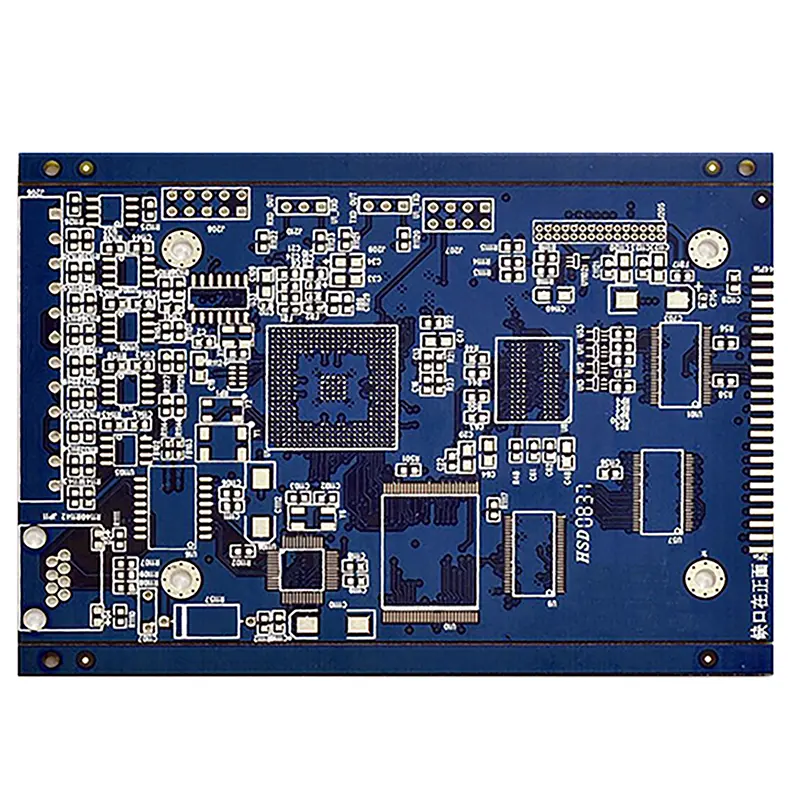 HDI PCB
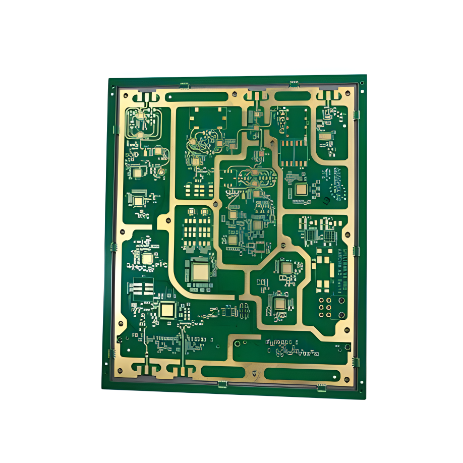 Rogers High-Frequency Board
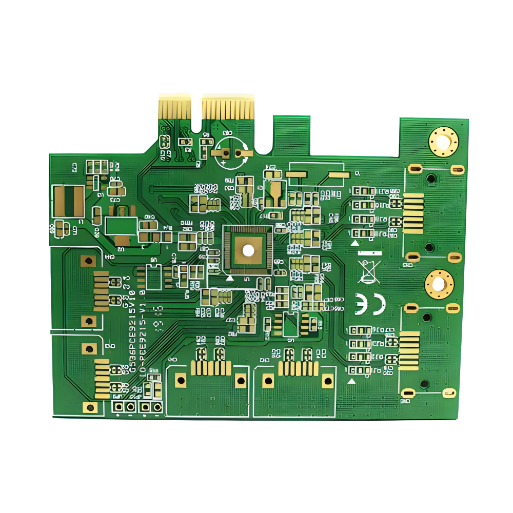 PTFE Teflon High-Frequency Board
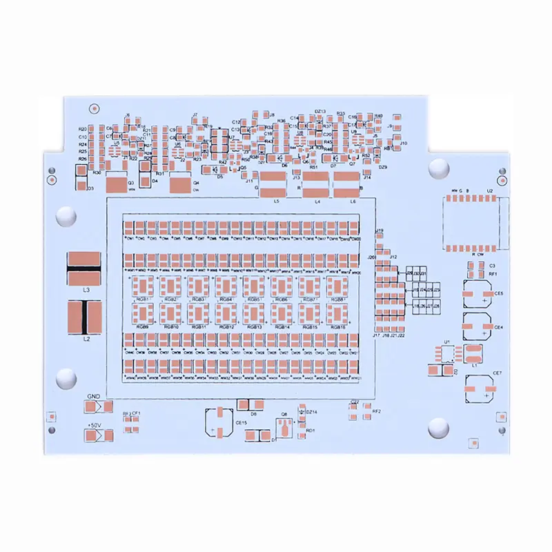 Aluminum
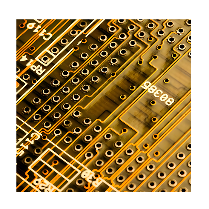 Copper Core
 PCB Assembly
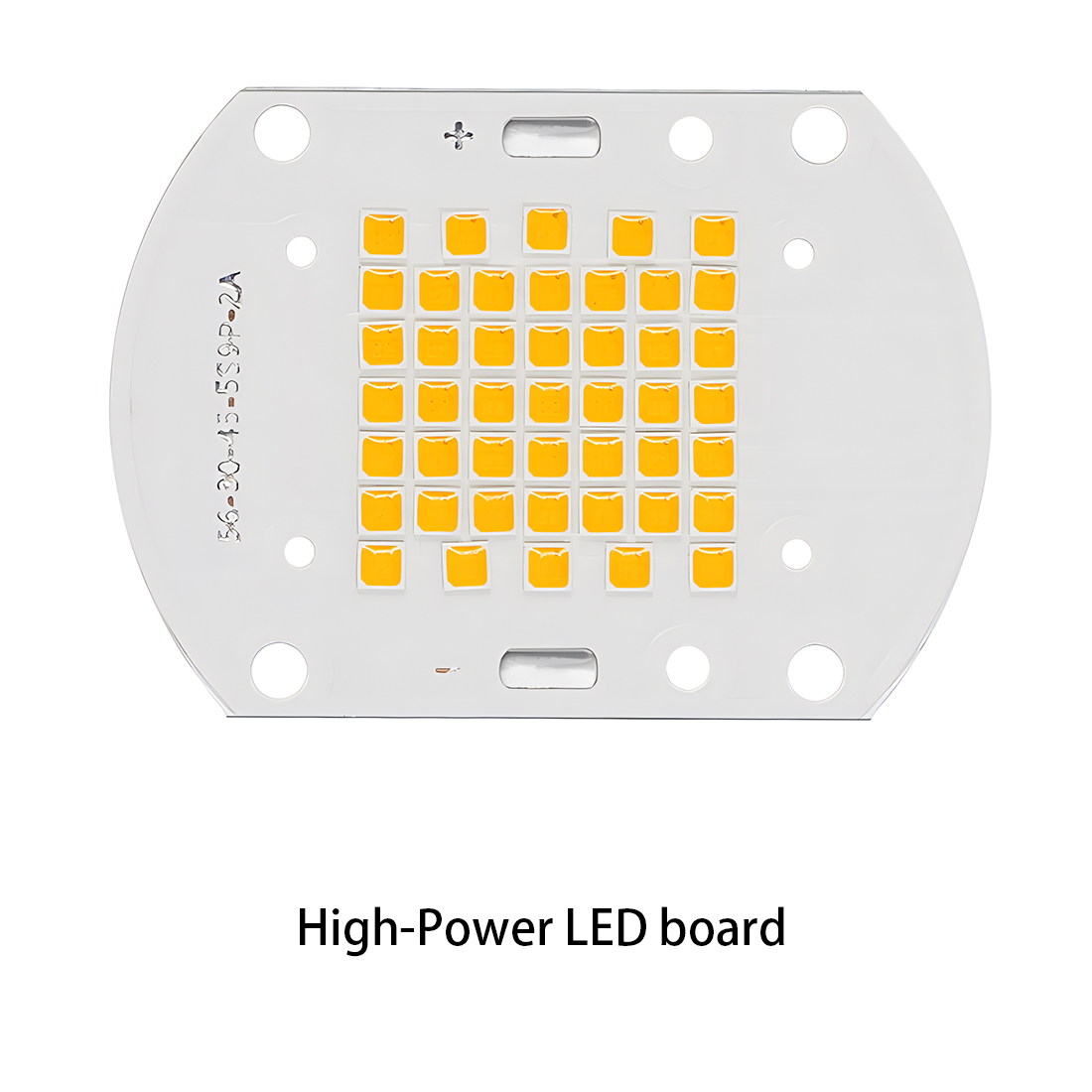 LED light PCBA
 Memory PCBA
 Power Supply PCBA
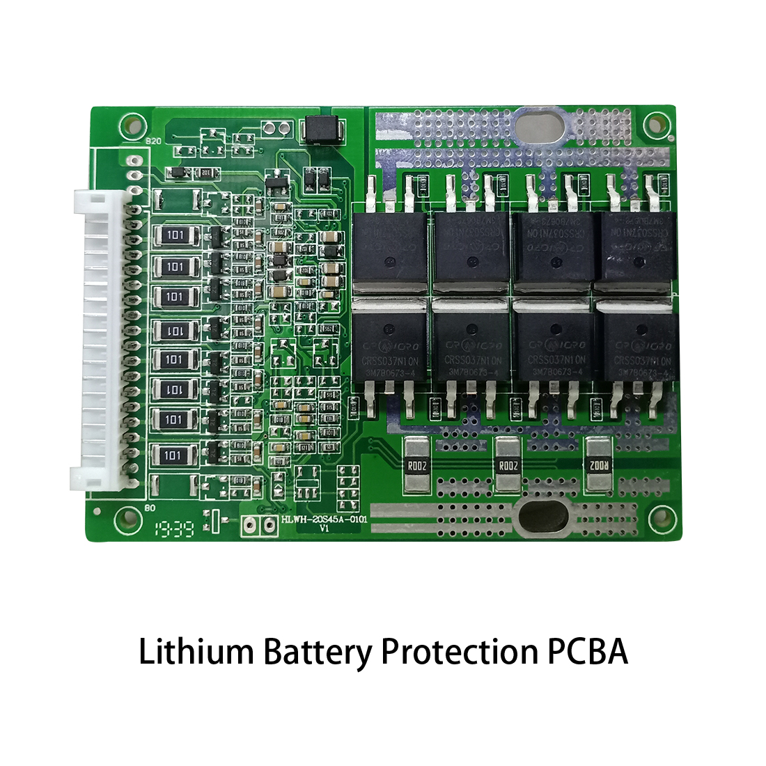 New Energey PCBA
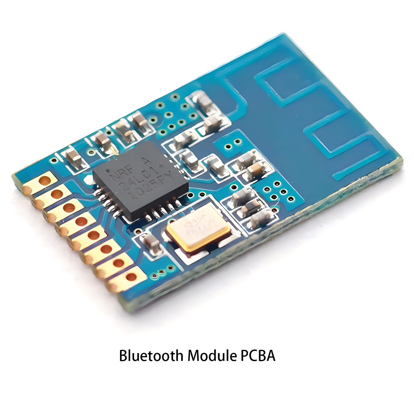 Communication PCBA
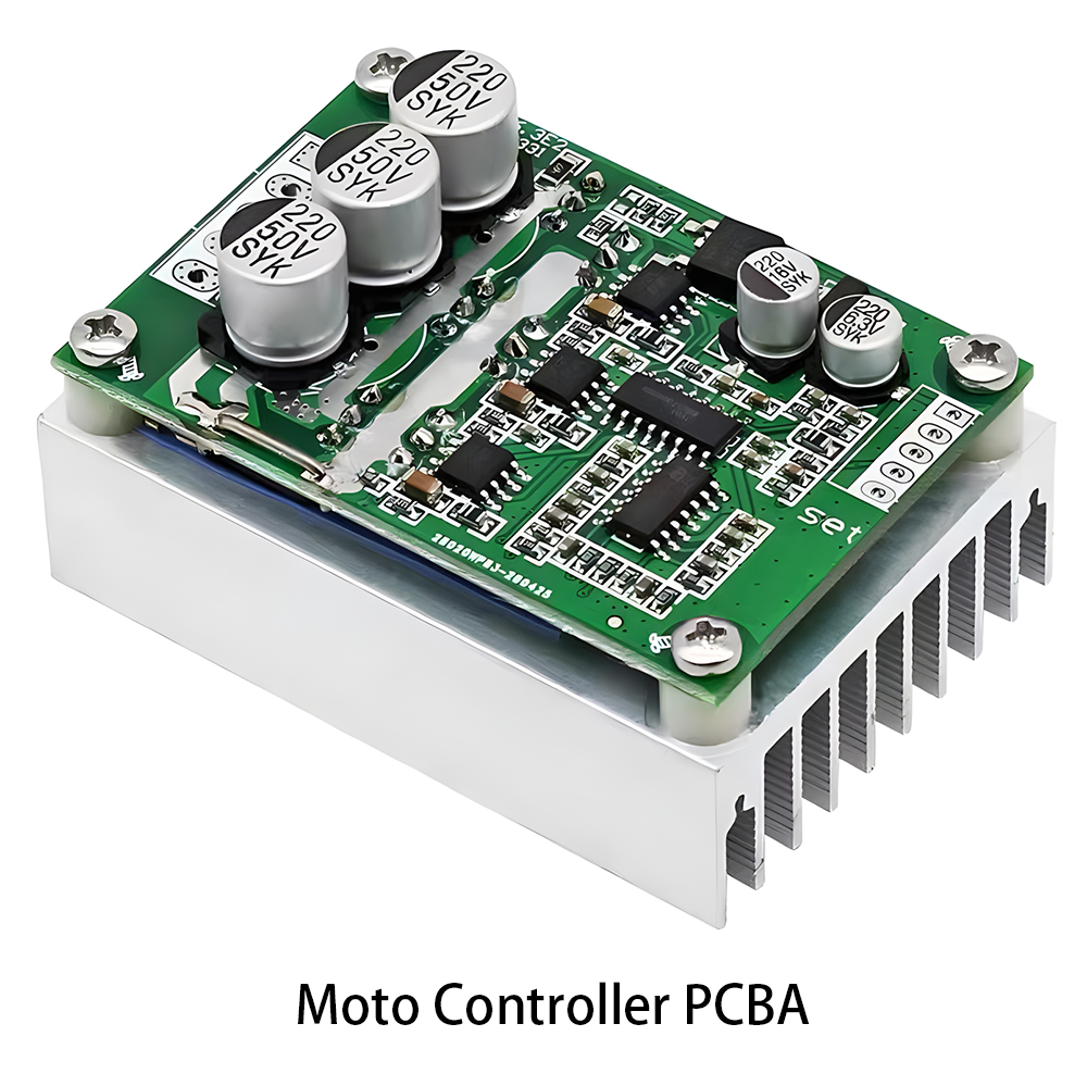 Industrial Control PCBA
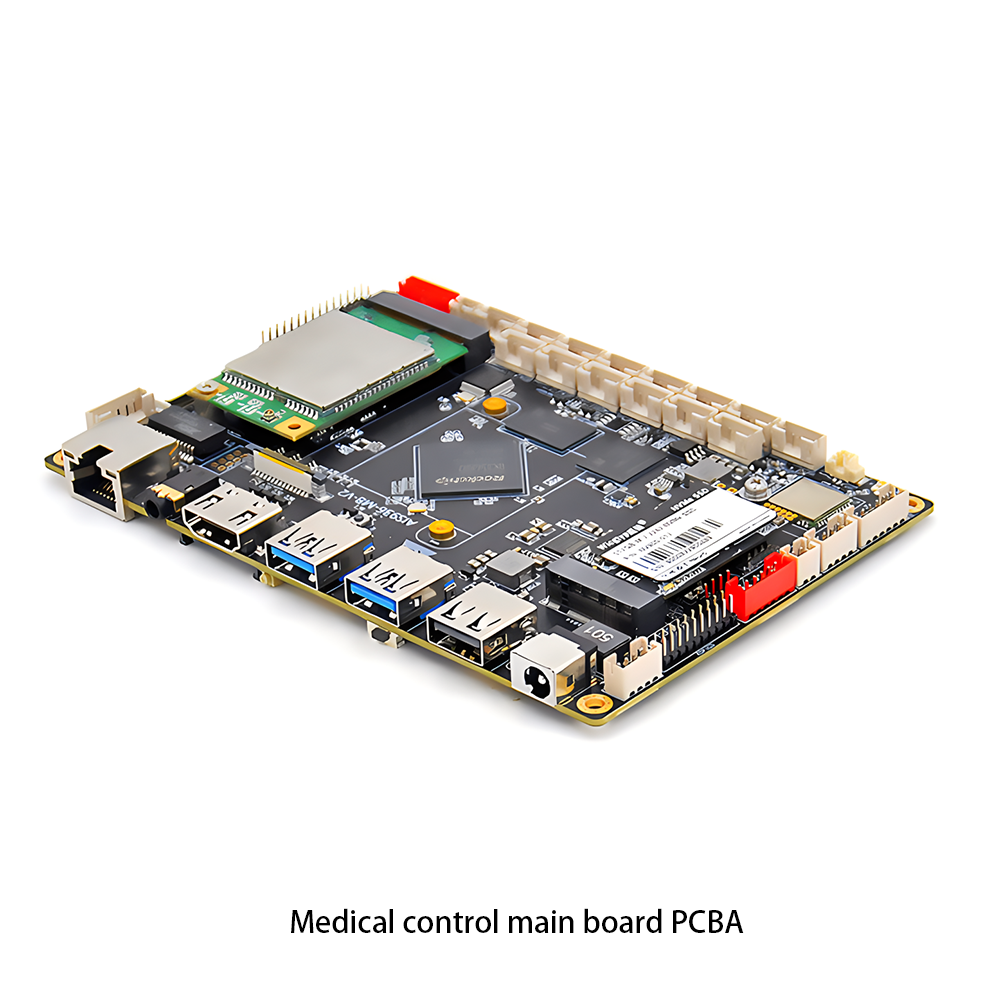 Medical Equipment PCBA
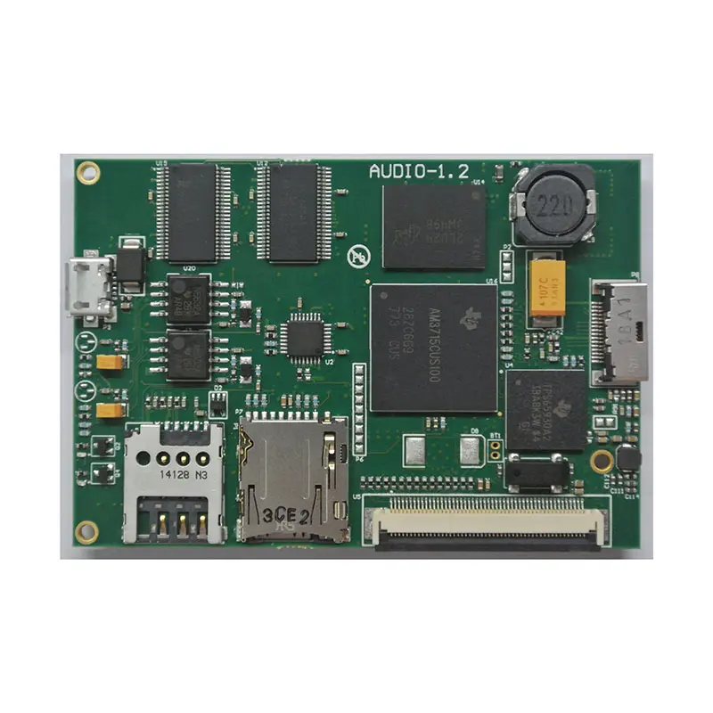 Testing Service
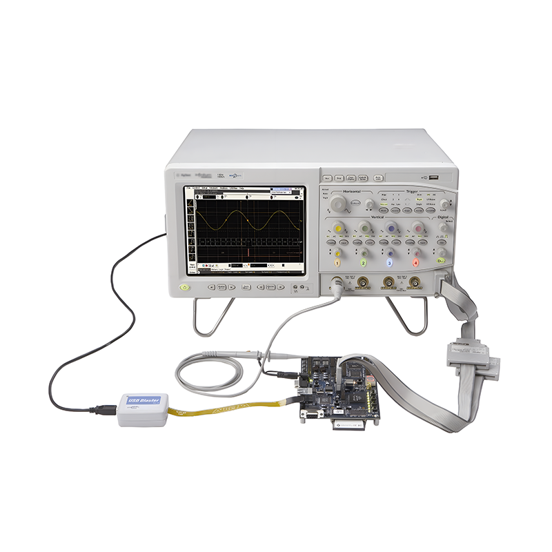 PCBA Testing Service
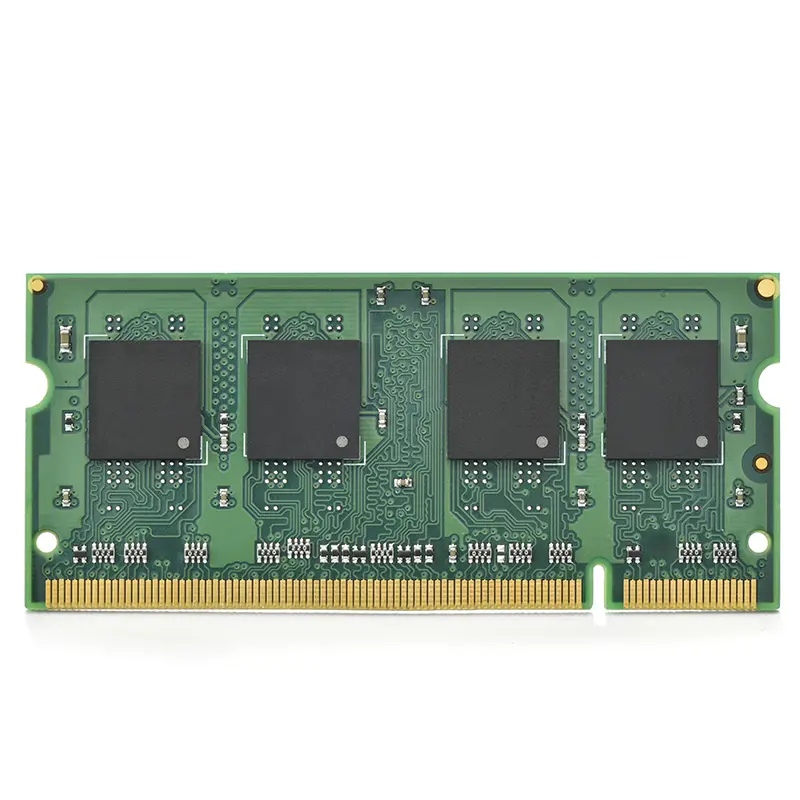 Certification Application
 RoHS Certification Application
 REACH Certification Application
 CE Certification Application
 FCC Certification Application
 CQC Certification Application
 UL Certification Application
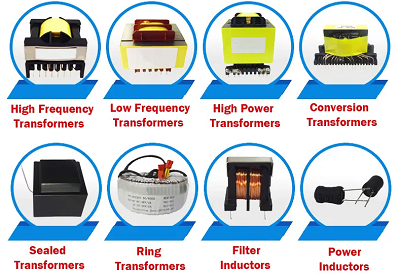 Transformers
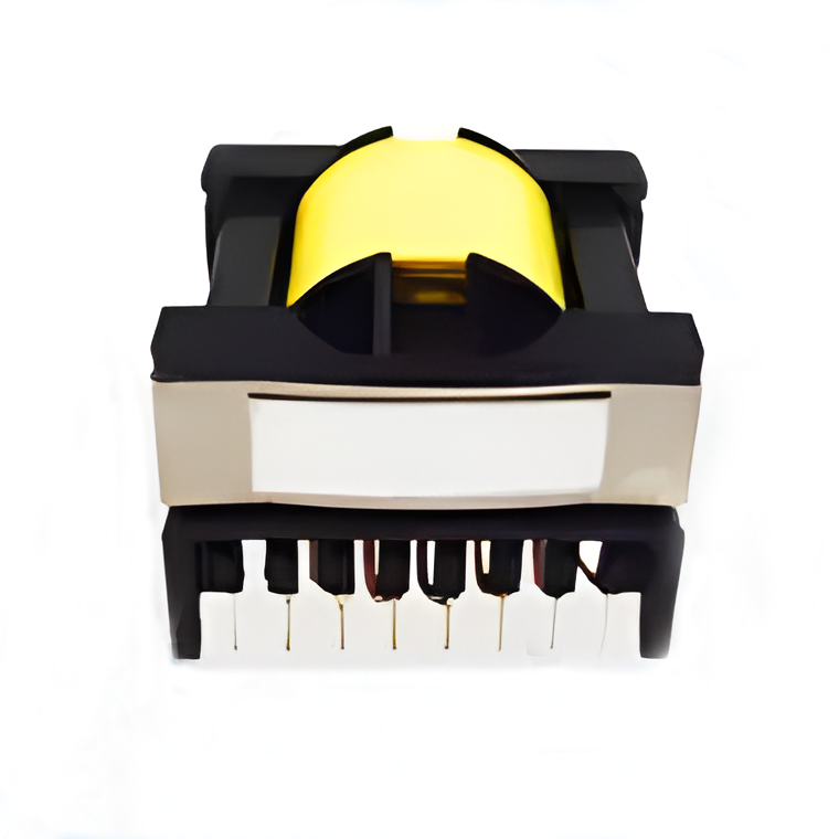 High Frequency Transformers
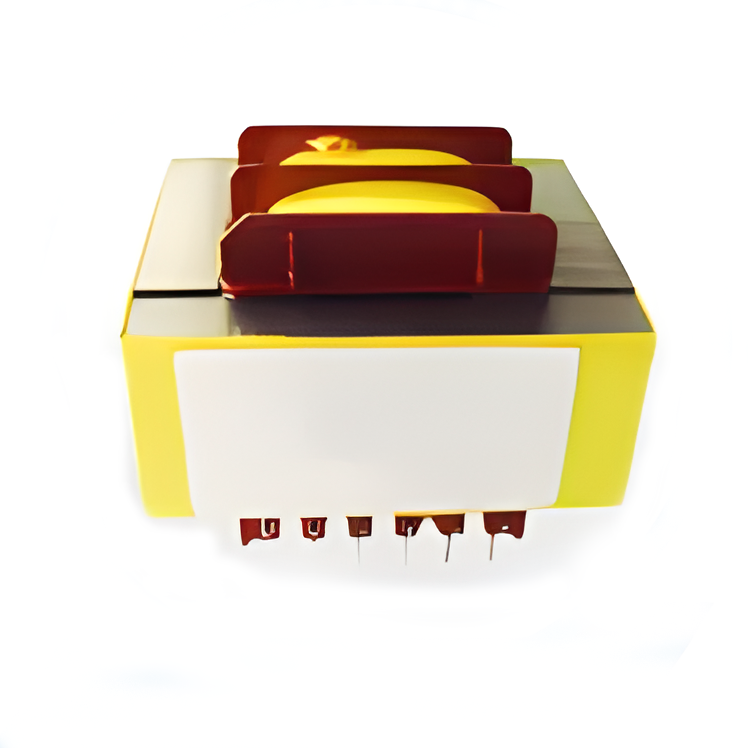 Low Frequency Transformers
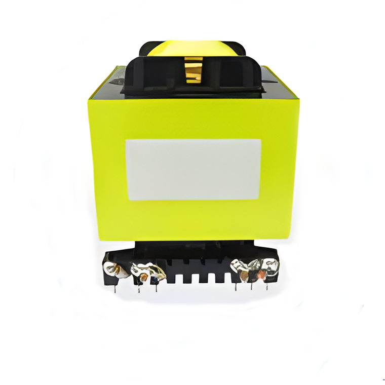 High Power Transformers
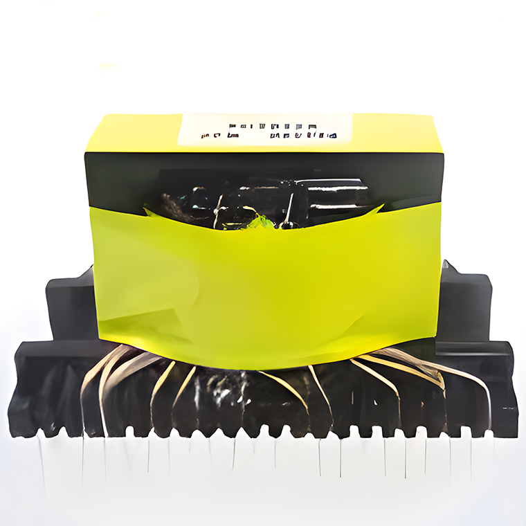 Conversion Transformers
 Sealed Transformers
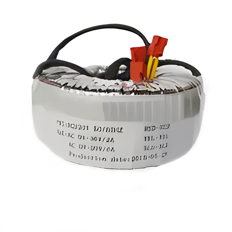 Ring Transformers
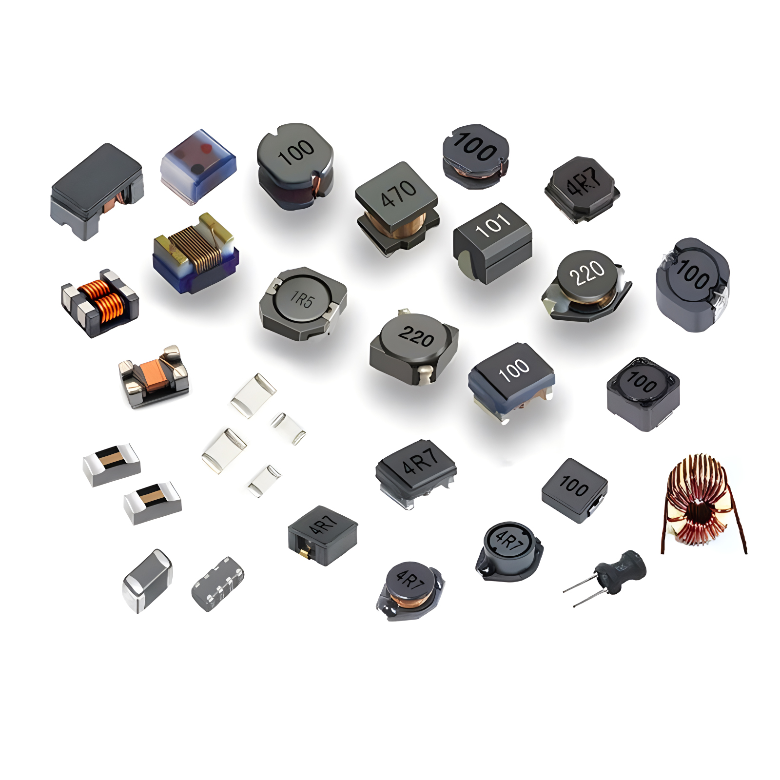 Inductors
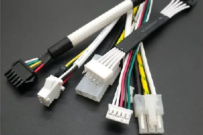 Wires,Cables Customized
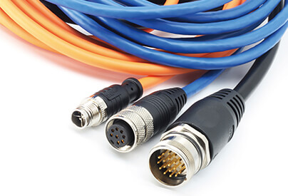 wires-cables
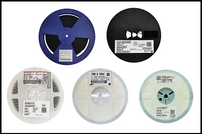 Components sourcing
High-speed PCB design guide: improving circuit design procedures to improve testability methods
Improving Circuit Design Procedures to Enhance Testability
With the increasing level of miniaturization, tremendous advancements have been made in component and wiring technology. For instance, the highly integrated micro ICs with BGA packaging and the reduction of insulation spacing between conductors to 0.5mm are just two examples. The way electronic components are wired has an increasingly significant impact on whether tests can be carried out effectively during subsequent production processes. Below are several important rules and practical tips.
By adhering to certain guidelines (DFT - Design for Testability), significant reductions in the preparation and implementation costs of production testing can be achieved. These guidelines have evolved over the years and, of course, they must be expanded and adapted accordingly as new production and component technologies are adopted. As the size of electronic products continues to shrink, two particularly noteworthy issues have emerged: the decreasing number of accessible circuit nodes and the limitations in applying methods such as In-Circuit-Test. To address these issues, corresponding measures can be taken in circuit layout, new testing methods can be adopted, and innovative adapter solutions can be utilized. The solution to the second issue also involves the additional tasks taken on by test systems that were originally used as independent processes. These tasks include programming memory components or implementing Built-in Self Test (BIST) through the test system. Transferring these steps to the test system creates more added value overall. To successfully implement these measures, corresponding considerations must be made during the product research and development phase.
1.What is Testability?
The meaning of testability can be understood as: the ability for test engineers to detect the characteristics of a component with the simplest methods possible to determine whether it meets expected functional requirements. In simpler terms:
- How simplified are the methods for detecting whether a product meets technical specifications?
- How quickly can test programs be developed?
- How comprehensive are the detections of product defects?
- How simplified are the methods for accessing test points?
To achieve good testability, both mechanical and electrical design guidelines must be considered. Of course, achieving optimal testability comes with a certain cost, but it brings a series of benefits to the entire production process and is an important prerequisite for successful product production.
-
Why Develop Test-Friendly Technology
In the past, if a product could not be tested at a previous test point, the issue was simply pushed to the next test point. If product defects could not be detected during production testing, the identification and diagnosis of these defects were also simply pushed to functional and system testing.
In contrast, today, people are trying to detect defects as early as possible, not only because of lower costs but also because today's products are so complex that some manufacturing defects may not be detected in functional testing. For example, this is the case for components that require pre-installed software or programming, such as flash memory or In-System Programmable Devices (ISPs). The programming of these components must be planned during the research and development phase, and the test system must also be capable of handling this programming.
While test-friendly circuit design requires some investment, the cost of designing a difficult-to-test circuit can be even higher. Testing itself has a cost, which increases with each additional level of testing, from in-circuit testing to functional testing and system testing. Skipping any of these tests can result in even greater costs. The general rule is that the cost of each additional level of testing increases by a factor of 10. By designing test-friendly circuits, faults can be detected earlier, which quickly offsets the cost of test-friendly circuit design. -
How do documents affect testability
Only by making full use of the complete data in component development can it be possible to develop a test program that can comprehensively detect faults. In many cases, close cooperation between the development and testing departments is necessary. Documentation has an undisputed impact on test engineers' understanding of component functionality and the development of testing strategies.
To bypass the problems caused by lack of documentation and limited understanding of component functionality, test system manufacturers can rely on software tools that automatically generate test patterns based on random principles, or rely on non-vector methods, which can only be considered a stopgap solution.
The complete documentation before testing includes a parts list, circuit design diagram data mainly in CAD format, and detailed information about the functions of the components, such as data sheets. Only by having all the information can one prepare test vectors, define component failure patterns, or perform certain pre-adjustments.
Certain mechanical data are also important, such as those required for checking the welding quality and positioning of components. Finally, for programmable components such as flash memory, PLD, FPGA, etc., if they are not programmed at the final installation, they should be programmed on the test system. The respective programming data must also be known. The programming data for flash components should be complete and intact. For example, if a flash chip contains 16Mbit of data, it should be able to use 16Mbit, which can prevent misunderstandings and avoid address conflicts. For example, if a 4Mbit memory is used to provide only 300Kbit of data to a component, this situation may occur. Of course, the data should be prepared in a popular standard format, such as Intel's Hex or Motorola's S record structure. Most test systems can interpret these formats as long as they can program flash or ISP components. Many of the information mentioned earlier are also necessary for component manufacturing. Of course, a clear distinction should be made between manufacturability and testability, as these are completely different concepts and thus constitute different premises. -
Good testability of mechanical contact conditions
If the basic rules of mechanics are not considered, even circuits with very good testability in electrical terms may be difficult to test. Many factors limit electrical testability. If the test points are not enough or too small, it may be difficult for the probe bed adapter to reach every node of the circuit. If the position error and size error of the test points are too large, it may lead to poor test repeatability. When using the probe bed adapter, it is important to pay attention to a series of recommendations regarding the size and positioning of the latching holes and test points. -
Electrical preconditions for optimal testability
Electrical prerequisites are as important as mechanical contact conditions for good testability, and both are essential. A gate circuit cannot be tested because it may not be able to access the start input through the test point, or the start input may be inside the package and cannot be accessed from the outside. In principle, both situations are equally bad and prevent testing from being carried out. When designing circuits, it should be noted that any component that requires online testing should have some mechanism to electrically isolate each component. This mechanism can be achieved by prohibiting the input terminal, which can control the output terminal of the component in a static high-ohmic state.
Although almost all test systems can bring the state of a node to any state by backdriving, it is best to have a node with a disable input to first bring the node to a high-impedance state and then "gently" add the corresponding level.
Similarly, the beat generator is always disconnected directly from the oscillator through a start-up lead, gate circuit, or plug-in bridge. The start-up input must never be directly connected to the circuit, but rather connected to the circuit through a 100 ohm resistor. Each component should have its own start-up, reset, or control pin. It is important to avoid having many components' start-up inputs share a resistor to connect to the circuit. This rule also applies to ASIC components, which should also have a pin through which the output can be brought to a high-ohm state. If the component can be reset when it is connected to operating voltage, this is also very helpful for resetting by a tester. In this case, the component can simply be placed in a specified state before testing.
The unused component pins should also be accessible, as undetected short circuits in these areas may also cause component failure. In addition, unused gate circuits are often used for design improvements in the future, and they may be reconnected to the circuit. Therefore, it is also important to test them from the beginning to ensure their reliability.
-
Improve testability
Suggestions for improving testability when using probe bed adapters
Secure the hole
-
Diagonal configuration
-
Positioning accuracy is ±0.05mm ±2mil
-
Diameter accuracy is ±0.076/-0mm +3/-0mil
-
The positioning accuracy relative to the test point is ±0.05mm ±2mil
-
The distance from the edge of the component should be at least 3mm
-
No through contact
Test points
- As square as possible
- The diameter of the test point should be at least 0.88mm 35mil
- The size accuracy of the test point is ±0.076mm ±3mil
- The accuracy of the interval between test points is ±0.076mm ±3mil
- The interval between test points should be as close to 2.5mm as possible
- Tin plating, the end face can be directly welded
- The distance from the edge of the component should be at least 3mm
- All test points should be possible on the back of the plug-in board
- The test points should be evenly distributed on the plug-in board
- Each node has at least one test point with 100% channel
- Test points are available for spare or unused gate circuits
- Multiple external test points of the power supply are distributed in different locations
Component identification
- The text of the logo is oriented in the same direction
- Clear identification of model, version, serial number and barcode
- The name of the component should be clearly visible and directly marked near the component as much as possible
-
About flash memory and other programmable components
The programming time for flash memory can sometimes be very long, up to 1 minute for large memories or memory banks. Therefore, it is not allowed to have reverse driving of other components at this time, otherwise the flash memory may be damaged. To avoid this situation, all components connected to the control lines of the address bus must be placed in a high-ohmic state. Similarly, the data bus must also be able to be placed in an isolated state to ensure that the flash memory is empty and ready for the next programming step.
There are some requirements for in-system programmable components ISP, such as products from companies like Altera, XilinX, and Lattuce, as well as other special requirements. In addition to ensuring the mechanical and electrical prerequisites for testability, it is also necessary to ensure the possibility of programming and verifying data. For Altera and Xilinx components, the Serial Vector Format SVF is used, which has recently become an industrial standard. Many test systems can program such components and use the input data in the Serial Vector Format SVF for testing signal generators. Programming these components through the Boundary-Scan-Kette JTAG will also program the Serial Vector Format. When collecting programming data, it is important to consider the entire component chain in the circuit, and not just restore the data to the component to be programmed.
During programming, the automatic test signal generator takes into account the entire component chain and connects other components into a bypass model. Conversely, Lattice requires data in JEDEC format and parallel programming through the usual input and output ports. After programming, the data is also used to check component functionality. The data provided by the development department should be as easy as possible for the test system to directly apply or can be applied through simple conversion. -
What should be paid attention to for boundary scan JTAG
Components composed of fine grids based on complex components provide test engineers with only a few accessible test points. It is still possible to improve testability at this time. For this, boundary scan and integrated self-test technology can be used to shorten test completion time and improve test effectiveness.
For development engineers and test engineers, a testing strategy based on boundary scan and integrated self-test technology will definitely increase costs. Development engineers must use IEEE-1149.1-standard boundary scan components in the circuit, and try to make the corresponding specific test pins accessible to test data input-TDI, test data output-TDO, test clock frequency-TCK, and test mode selection-TMS as well as ggf. Test reset. Test engineers develop a boundary scan model BSDL-boundary scan description language for components. At this time, he must know what boundary scan functions and instructions the component supports. Boundary scan testing can diagnose short circuits and open circuits up to the pin level. In addition, if the development engineer has made provisions, automatic testing of components can be triggered by the boundary scan instruction "RunBIST". Especially when there are many ASICs and other complex components in the circuit, there is no usual test model for these components. By using boundary scan components, the cost of developing test models can be greatly reduced.
The degree of time and cost reduction varies for each component. For a circuit with an IC, if 100% discovery is required, approximately 400,000 test vectors are needed. By using boundary scan, the number of test vectors can be reduced to hundreds at the same fault discovery rate. Therefore, boundary scan method has particular advantages under the condition of no test model or limited access to circuit nodes. Whether to adopt boundary scan depends on the increased cost during development, utilization, and manufacturing. Boundary scan must be weighed against the time required for fault discovery, testing time, time to market, and adapter costs, and should be saved as much as possible. In many cases, a hybrid solution of traditional online testing methods and boundary scan methods is the best solution.