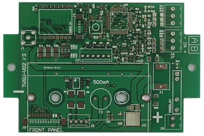
 PCB
PCB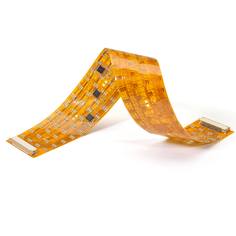 FPC
FPC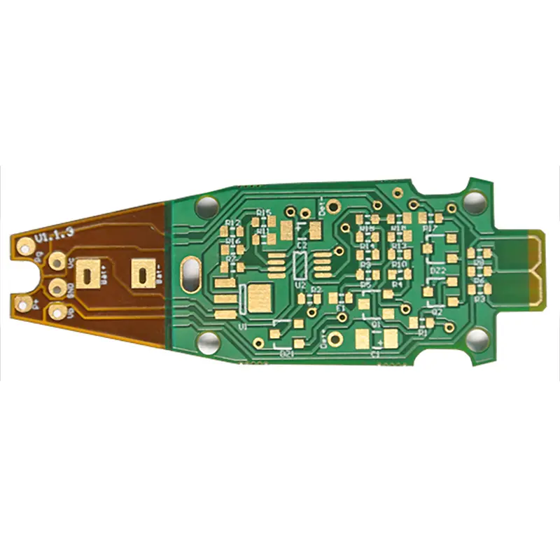 Rigid-Flex
 FR-4
FR-4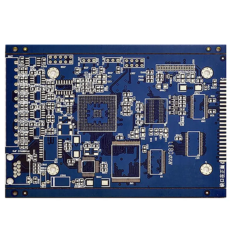 HDI PCB
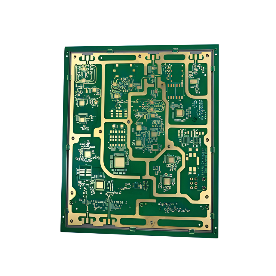 Rogers High-Frequency Board
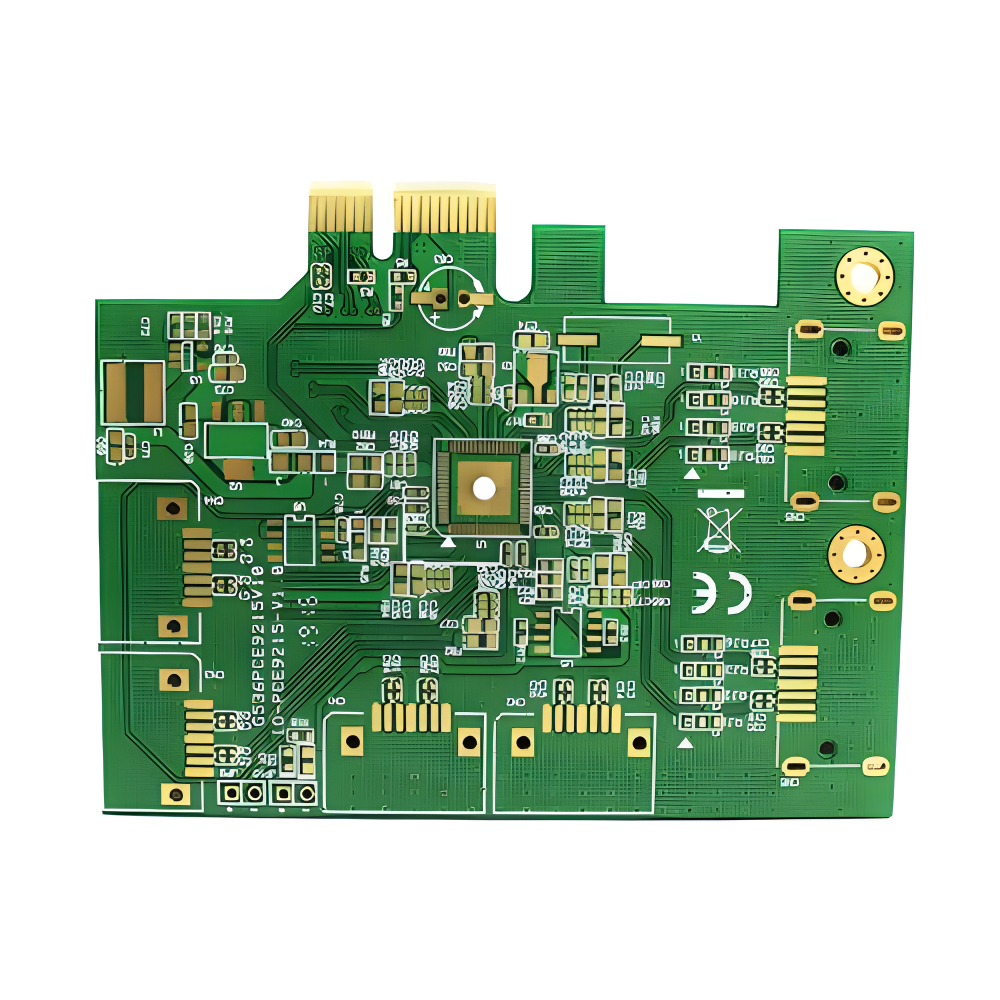 PTFE Teflon High-Frequency Board
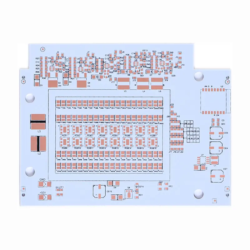 Aluminum
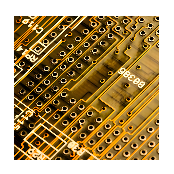 Copper Core
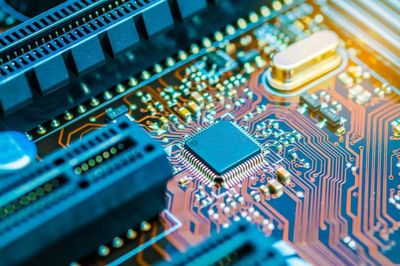 PCB Assembly
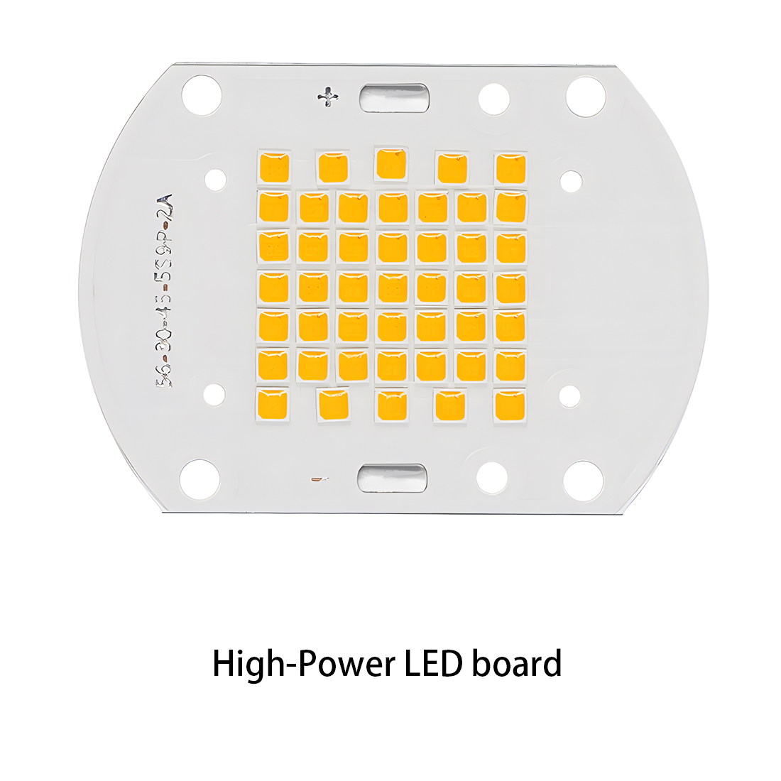 LED light PCBA
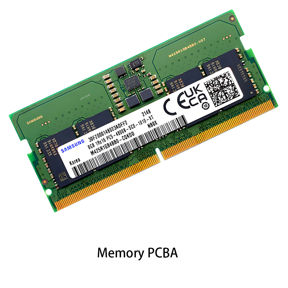 Memory PCBA
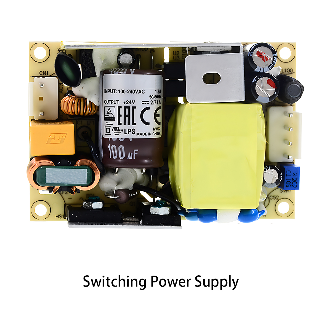 Power Supply PCBA
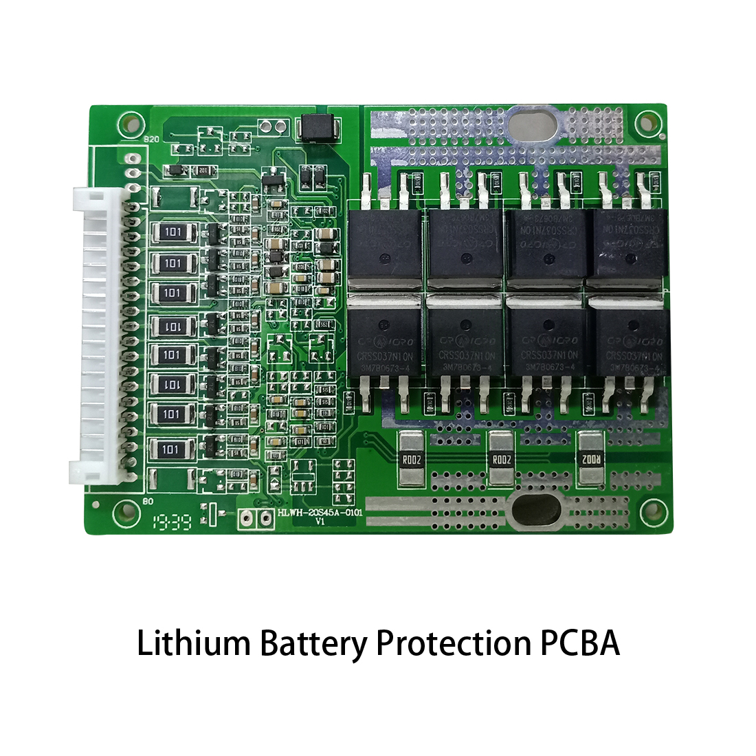 New Energey PCBA
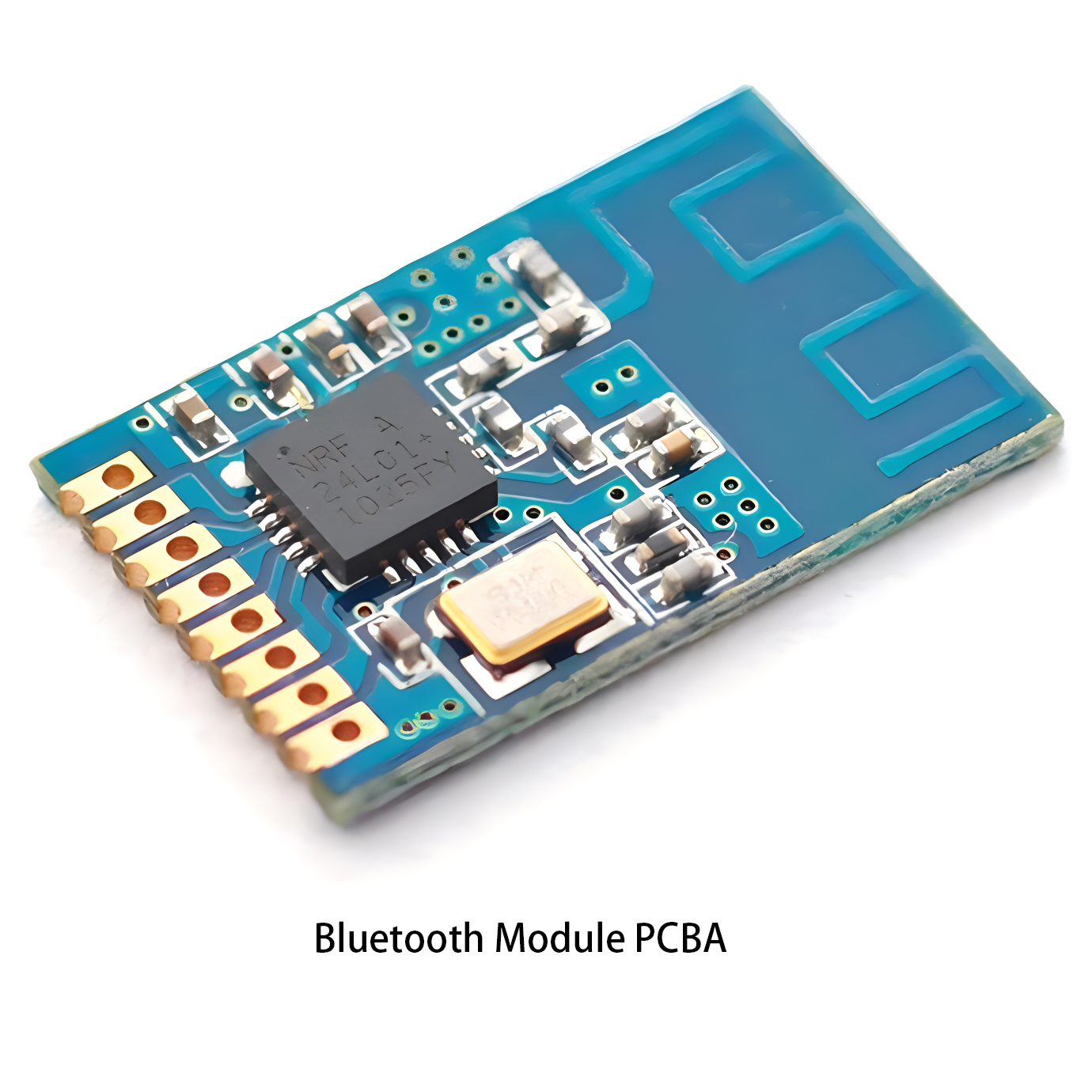 Communication PCBA
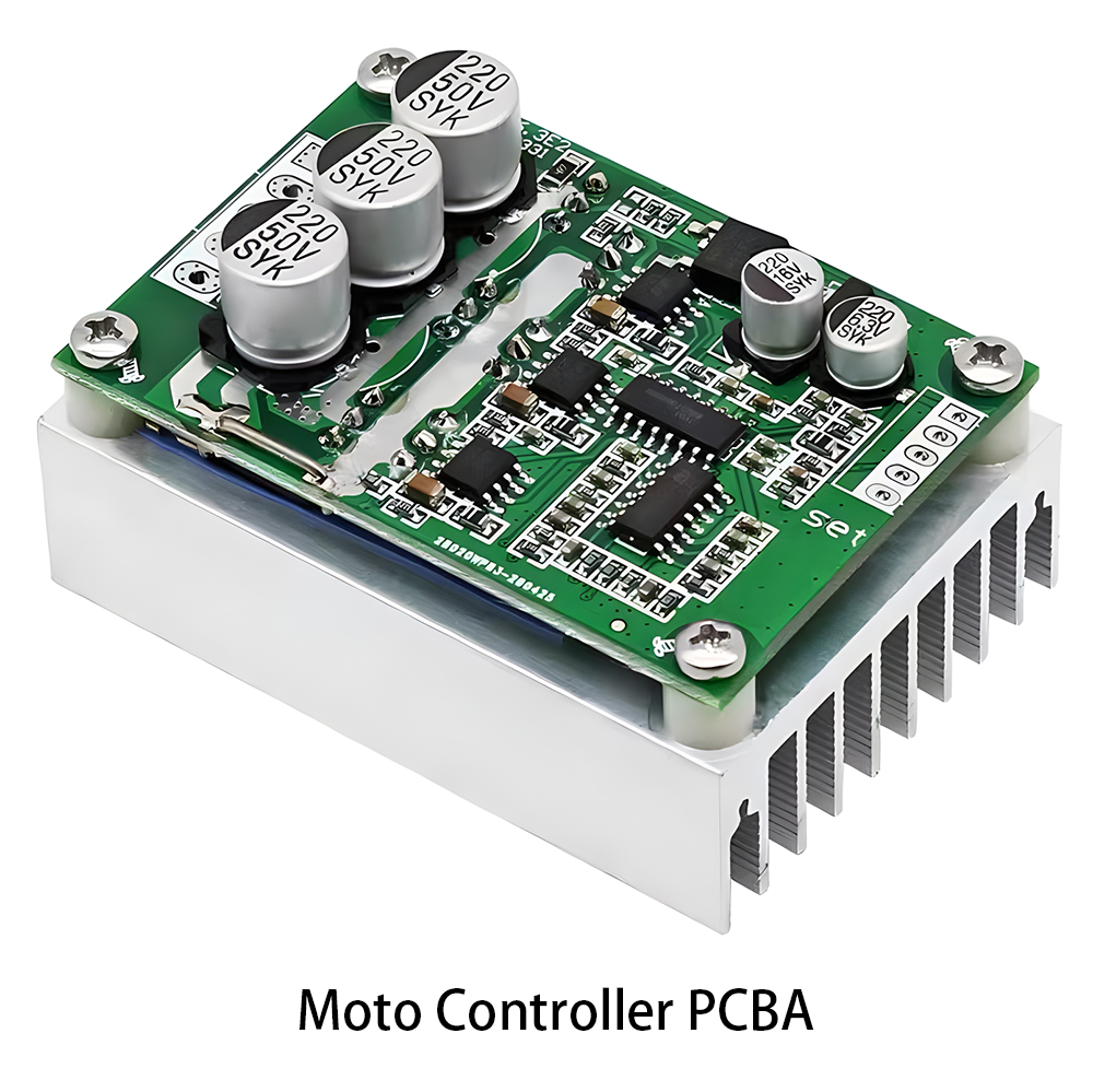 Industrial Control PCBA
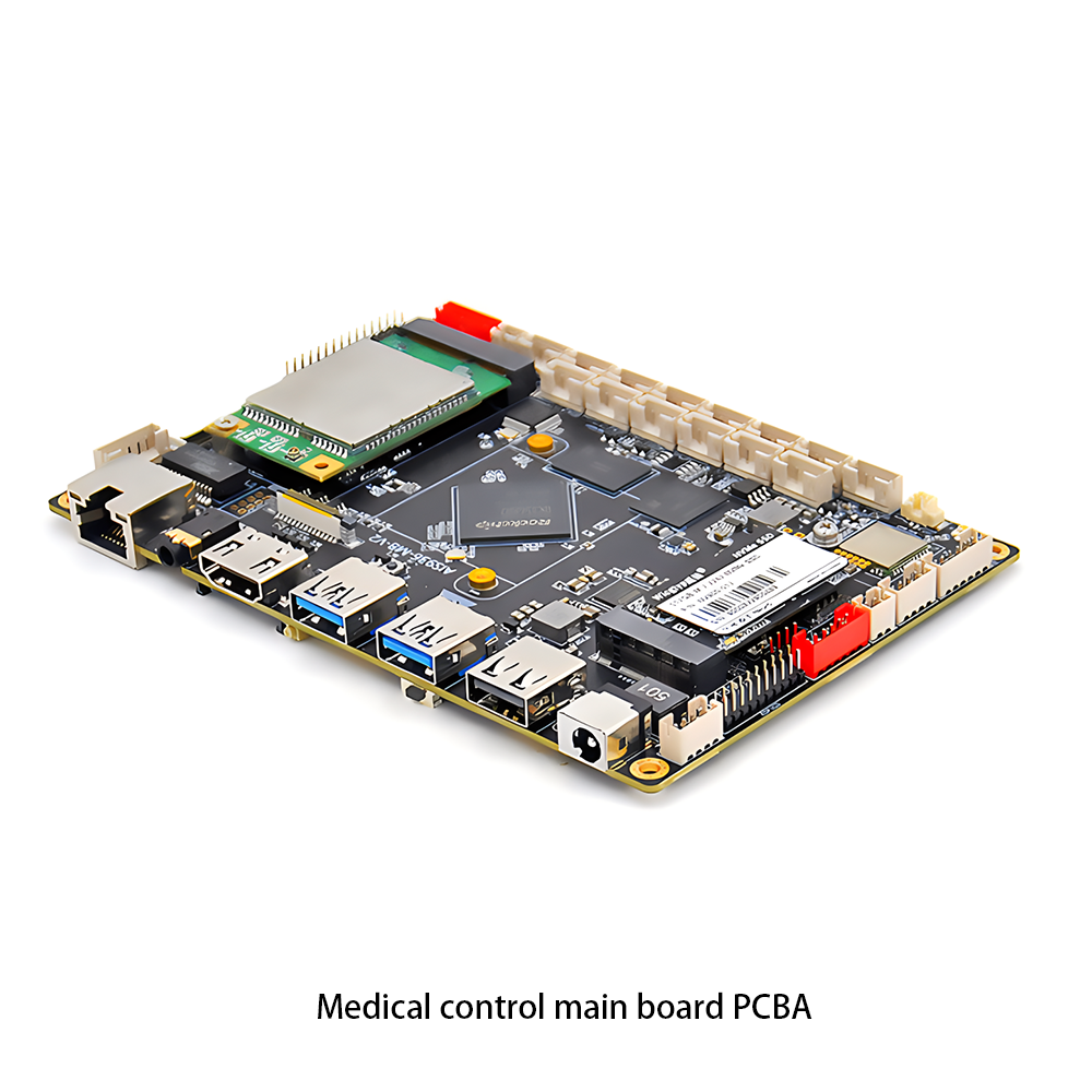 Medical Equipment PCBA
 Product Rebuild
 PCB Copy
 IC Cracking
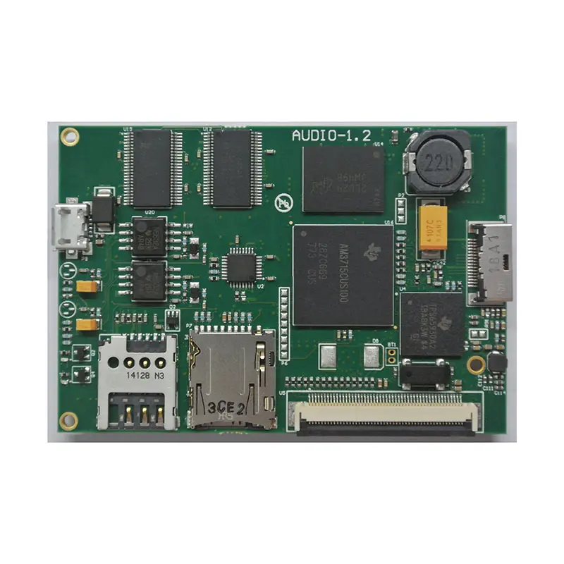 Testing Service
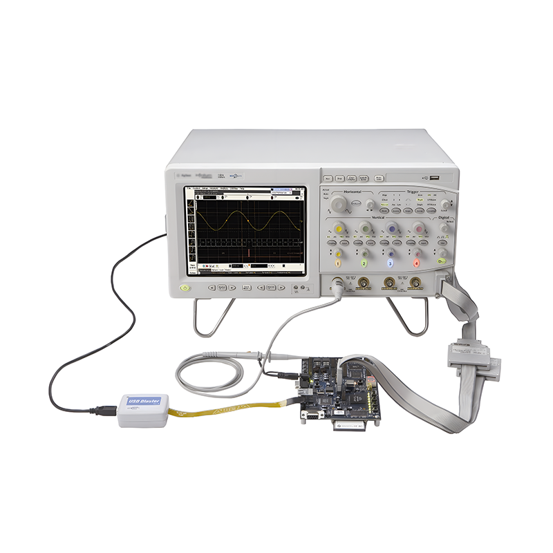 PCBA Testing Service
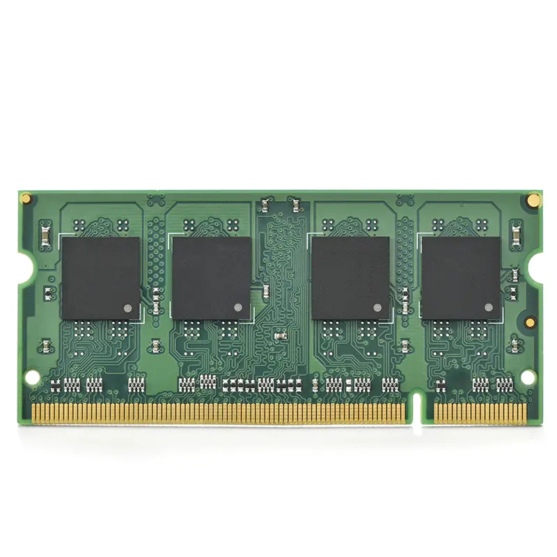 Certification Application
 RoHS Certification Application
 REACH Certification Application
 CE Certification Application
 FCC Certification Application
 CQC Certification Application
 UL Certification Application
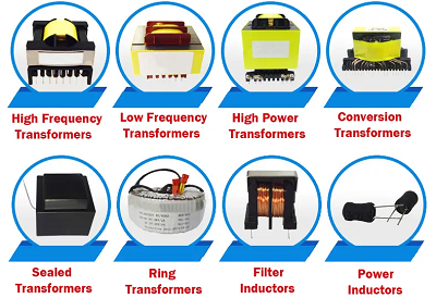 Transformers, Inductors
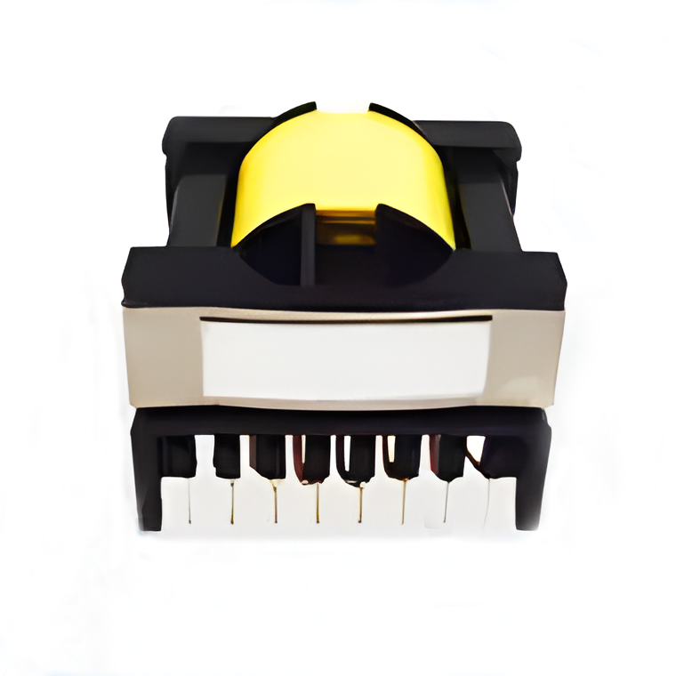 High Frequency Transformers
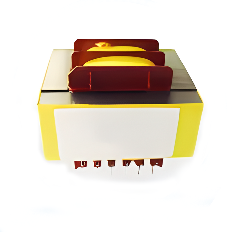 Low Frequency Transformers
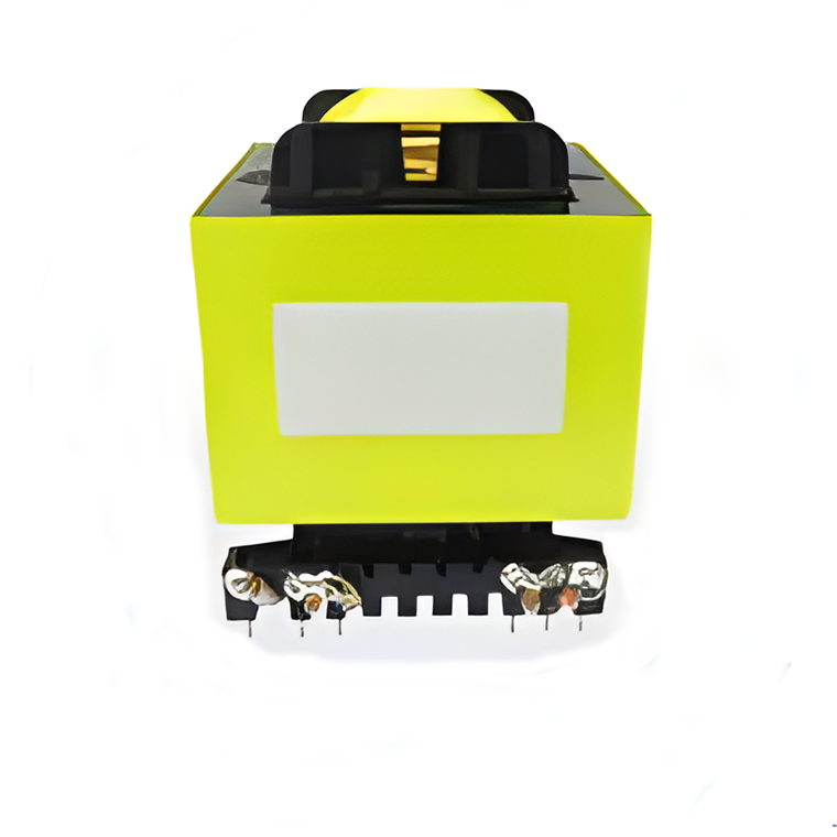 High Power Transformers
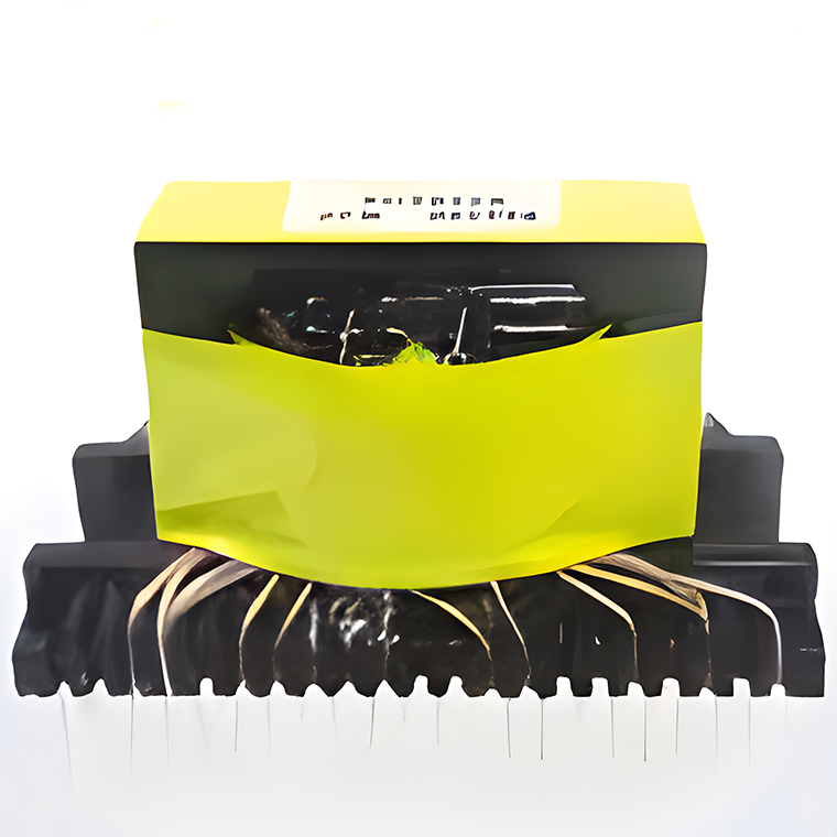 Conversion Transformers
 Sealed Transformers
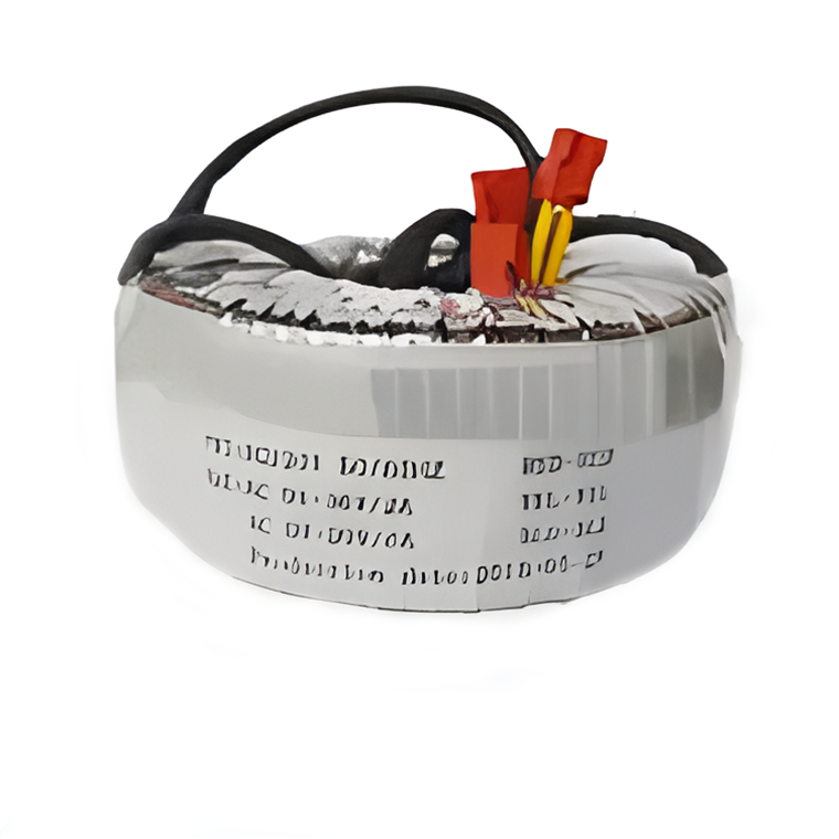 Ring Transformers
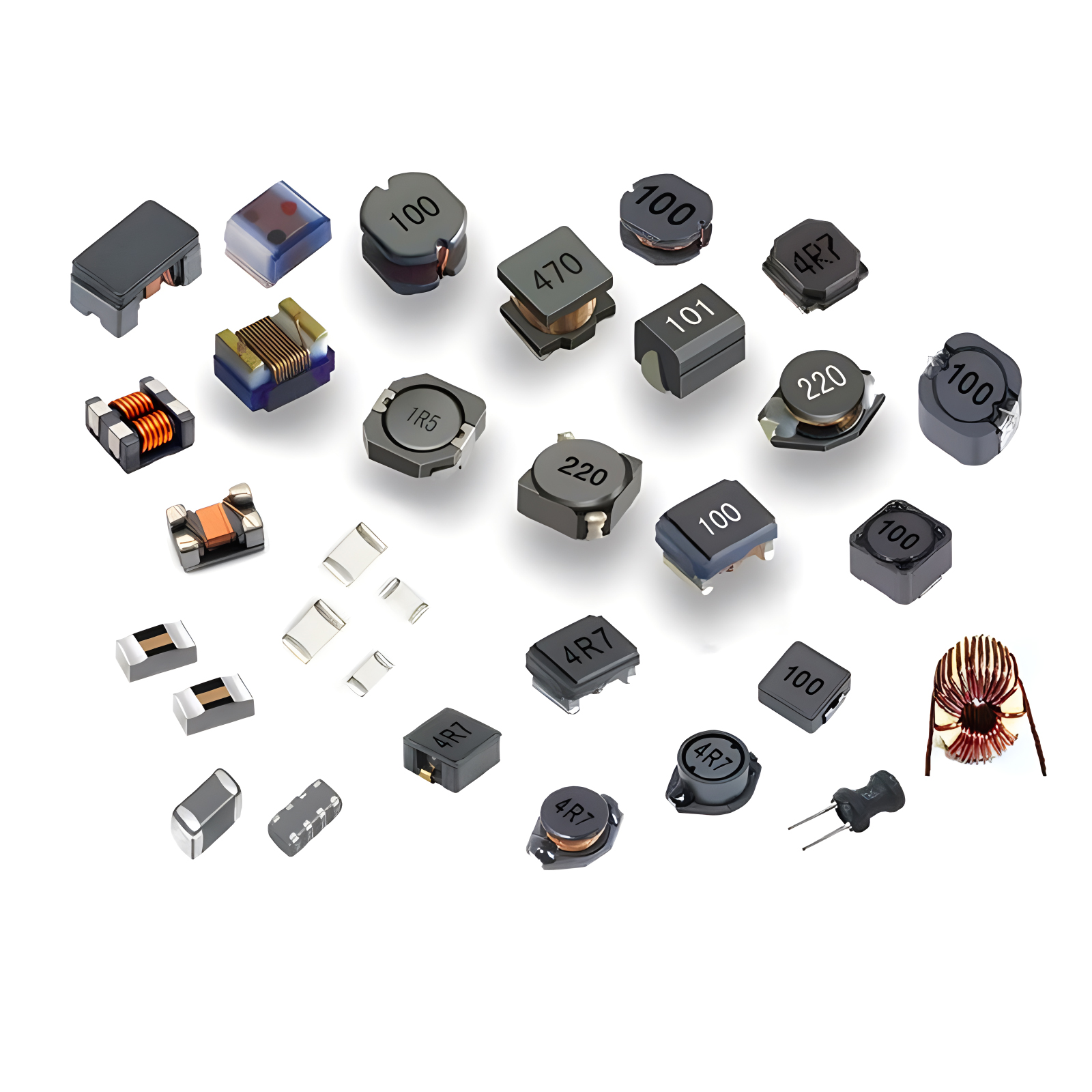 Inductors
 Wires,Cables Customized
 Network Cables
 Power Cords
 Antenna Cables
 Coaxial Cables
 Capacitors
 Connectors
 Diodes
 Embedded Processors & Controllers
 Digital Signal Processors (DSP/DSC)
 Microcontrollers (MCU/MPU/SOC)
 Programmable Logic Device(CPLD/FPGA)
HDI PCB: A Pioneer in Miniaturizing Electronic Devices and Enhancing High-Performance
HDI PCB: A Pioneer in Miniaturizing Electronic Devices and Enhancing High-Performance
In today's electronic era, where the pursuit of ultimate thinness and high performance coexist, HDI PCB (High-Density Interconnect PCB) has emerged as a cutting-edge technology that is gradually becoming an indispensable core component in various electronic devices. HDI PCB, with its unique advantages, has not only driven the miniaturization of components and semiconductor packages but also significantly enhanced the functional density and electrical performance of circuit boards.

The Precision Art of Design and Manufacturing
The essence of HDI PCB design lies in its ultra-fine circuit layout, tiny vias, and ultra-high wiring density. These characteristics enable HDI PCB to effortlessly handle the demands of chips with dense pins and complex functions in mobile devices, wearable devices, and other high-tech products. Compared to traditional PCBs, HDI PCB focuses more on compact component arrangement and circuit refinement, achieving the integration of more functions within limited space.
In terms of manufacturing, HDI PCB adopts advanced laser drilling technology, replacing the traditional mechanical drilling method. This transformation not only significantly reduces the via diameter range (down to 3.0-6.0mil) but also greatly improves drilling accuracy and efficiency. Smaller vias mean saved space for landing pads and increased layout density, bringing more possibilities and flexibility to circuit board design.

Notable Advantages and Widespread Applications
The advantages of HDI PCB are not limited to its design and manufacturing but also evident in its practical applications. Firstly, its compact design significantly optimizes circuit board space. Even complex 8-layer through-hole PCBs can be simplified into 4-layer HDI PCBs with equivalent functions, effectively reducing the overall size and weight of products.
Secondly, HDI PCB excels in signal integrity. The design of small vias reduces stray capacitances and inductances, while the combination of blind vias and via-in-pad technology helps shorten signal path lengths. This results in faster signal transmission and better signal quality, crucial for modern electronic devices that demand high-speed data transmission and low latency response.
Moreover, HDI PCB boasts high reliability. In harsh working environments, HDI technology ensures stable operation and long-term durability of circuit boards, providing reliable support for critical fields such as medical devices, aerospace, and more.
From a cost-effectiveness perspective, HDI PCB also has its merits. Although the initial investment may be slightly higher than traditional PCBs, as the number of layers and functionality increase, the cost advantages of HDI technology become apparent. Especially when producing circuit boards with more than 8 layers, HDI technology can significantly reduce manufacturing costs while maintaining functional requirements.

Minintel: Your Trusted HDI PCB Solution Provider
As a leader in the HDI PCB industry, Minintel is committed to enhancing equipment and employee expertise to meet customers' demands for high-quality, high-performance PCB products. Equipped with advanced production facilities and a professional technical team, we offer one-stop HDI PCB solutions from design to manufacturing. Whether for portable devices like smartphones and tablets, medical equipment, automotive devices, or military and aerospace applications, Minintel provides satisfactory HDI PCB products and services.
In the future, Minintel will continue to uphold the ideals of innovation and excellence, driving the development and application of HDI PCB technology, and contributing to the progress of the electronics industry.