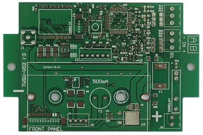
 PCB
PCB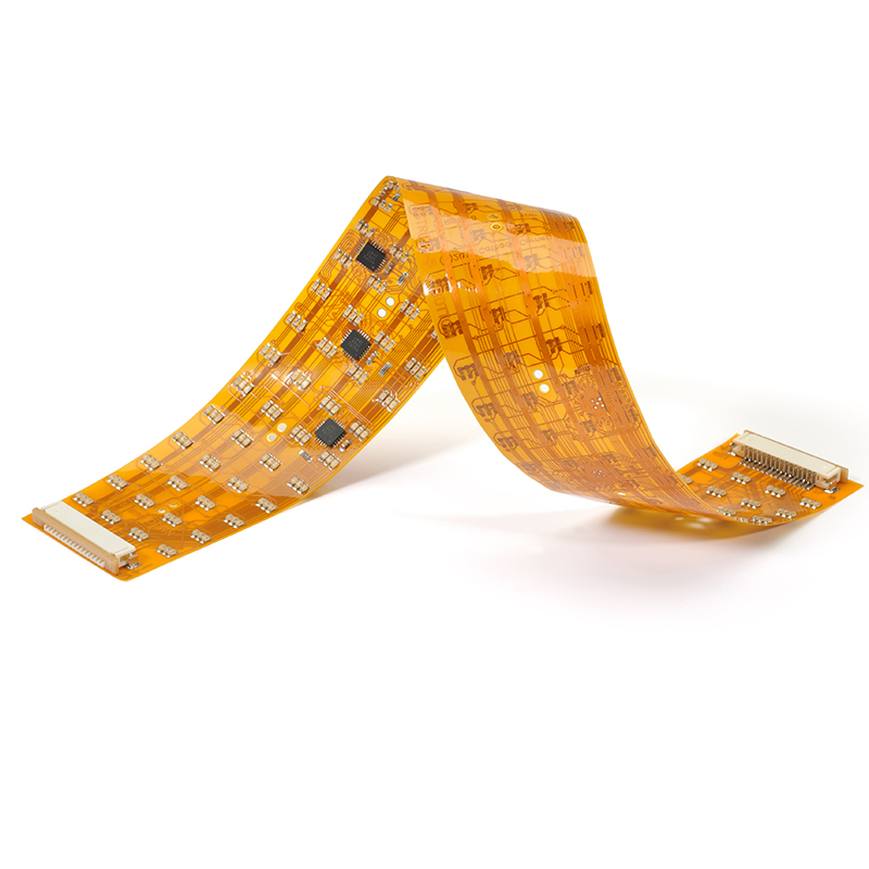 FPC
FPC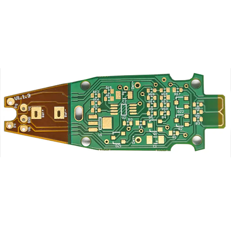 Rigid-Flex
 FR-4
FR-4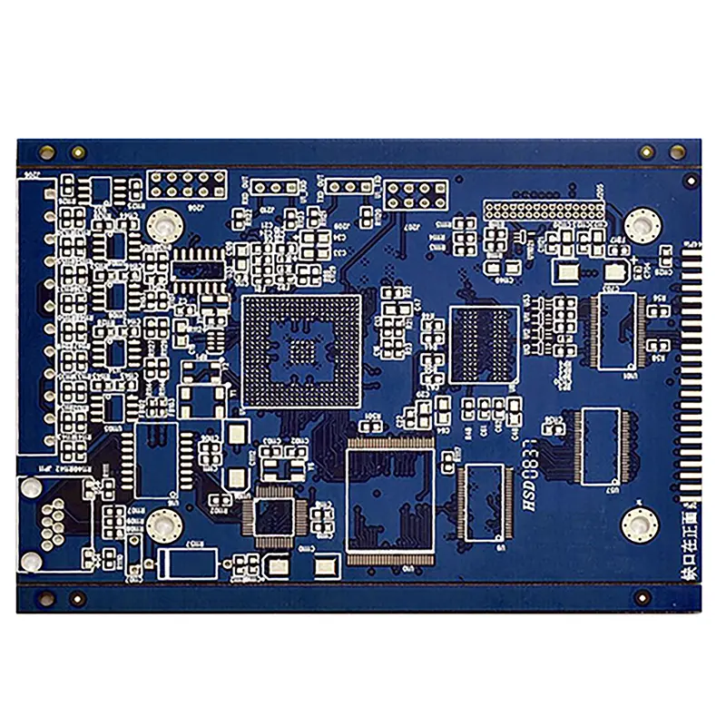 HDI PCB
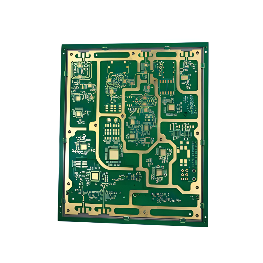 Rogers High-Frequency Board
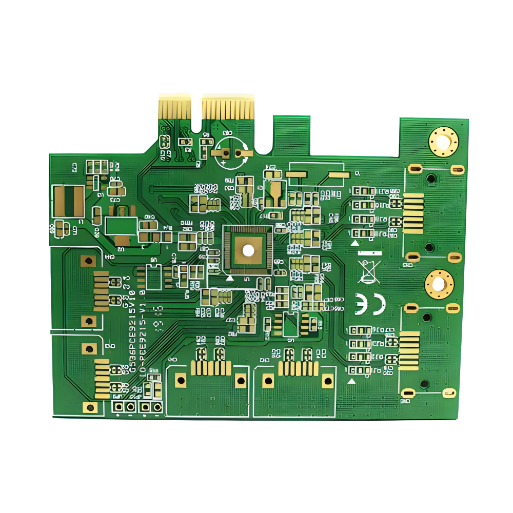 PTFE Teflon High-Frequency Board
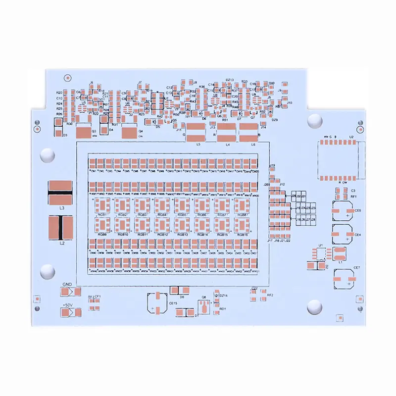 Aluminum
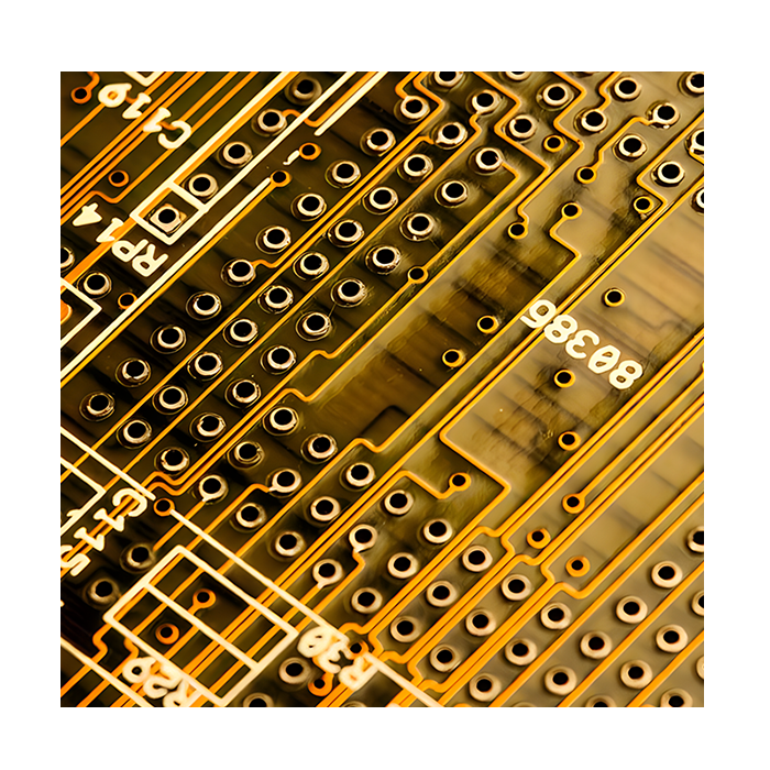 Copper Core
 PCB Assembly
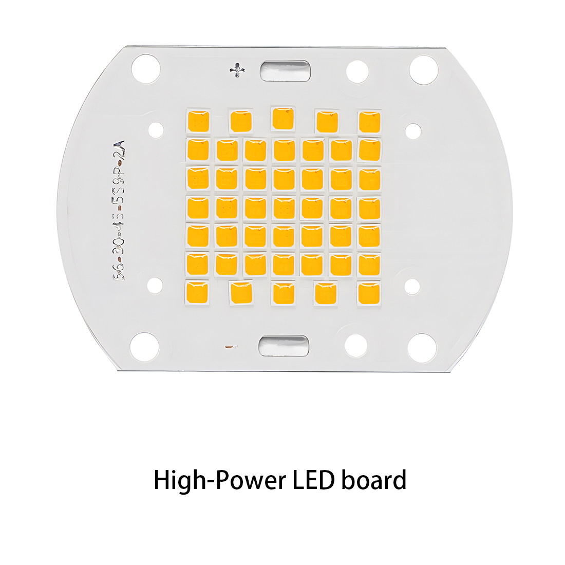 LED light PCBA
 Memory PCBA
 Power Supply PCBA
 New Energey PCBA
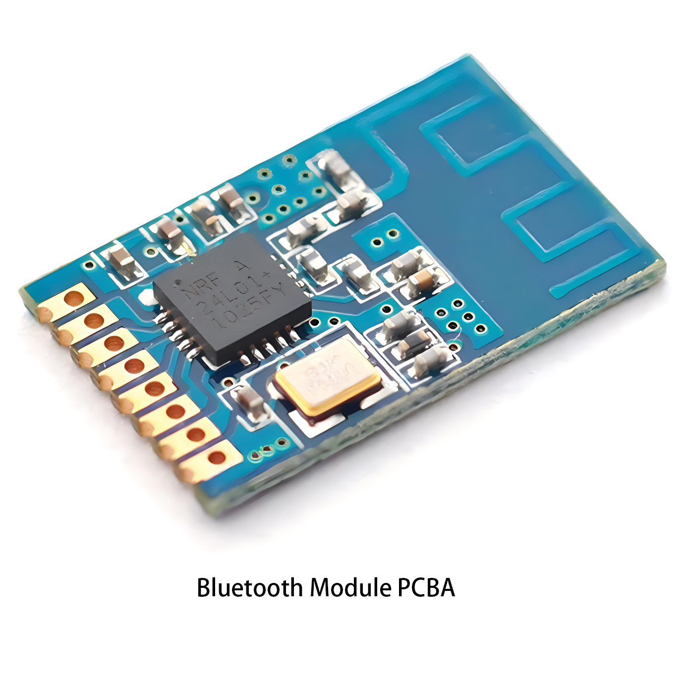 Communication PCBA
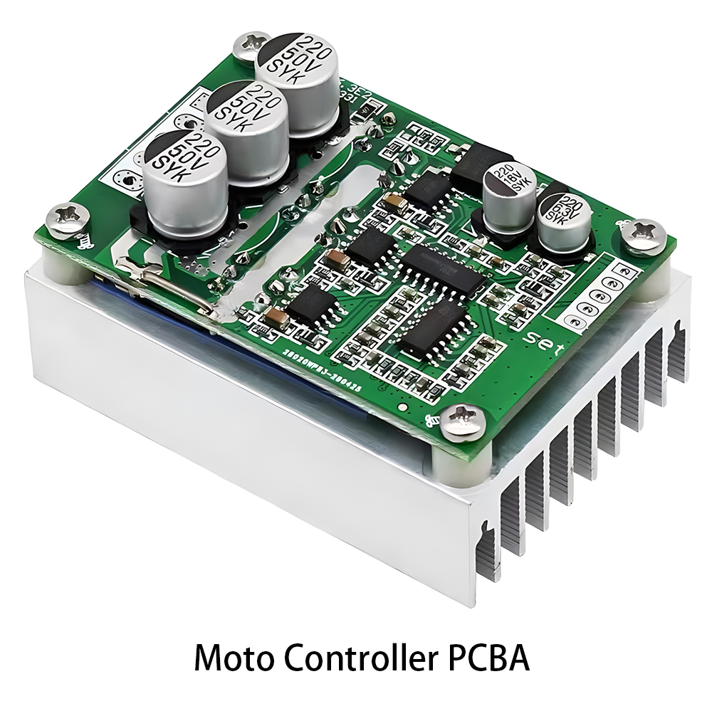 Industrial Control PCBA
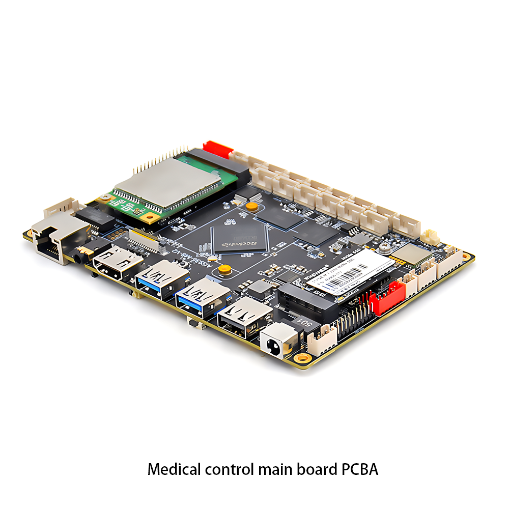 Medical Equipment PCBA
 Product Rebuild
 PCB Copy
 IC Cracking
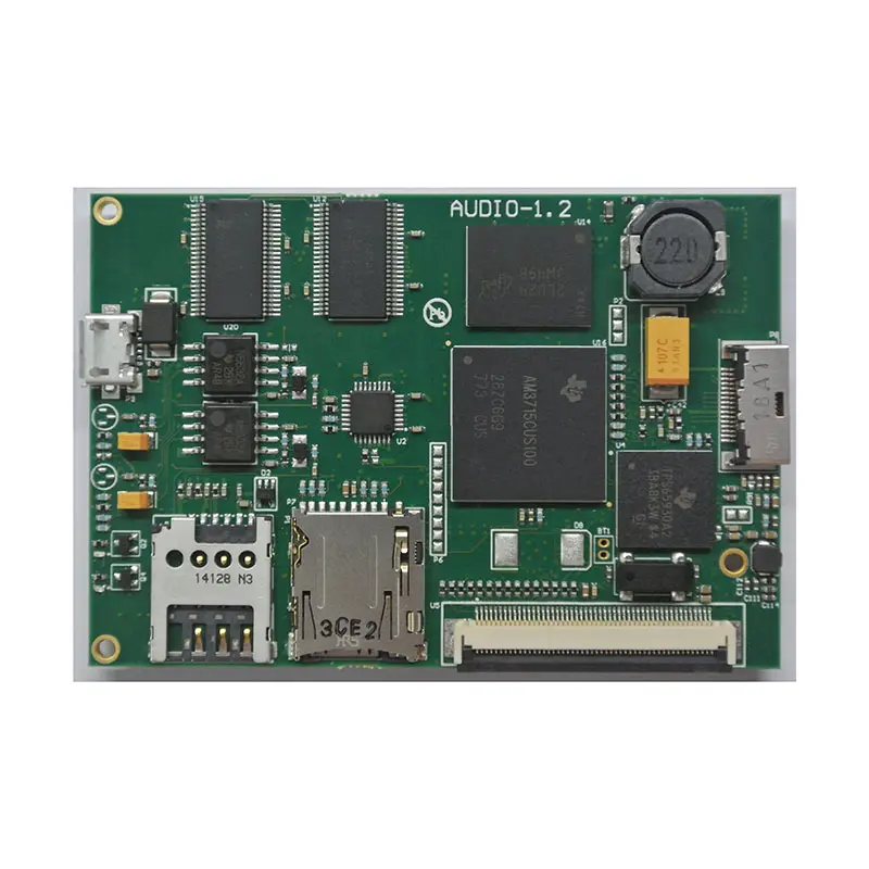 Testing Service
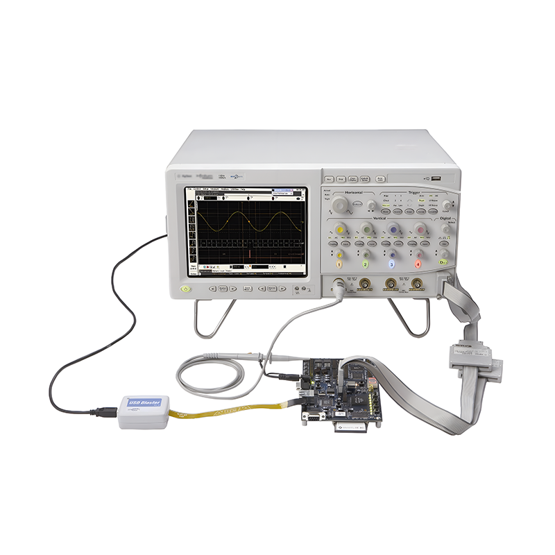 PCBA Testing Service
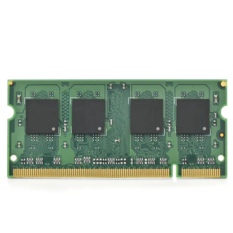 Certification Application
 RoHS Certification Application
 REACH Certification Application
 CE Certification Application
 FCC Certification Application
 CQC Certification Application
 UL Certification Application
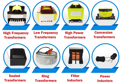 Transformers, Inductors
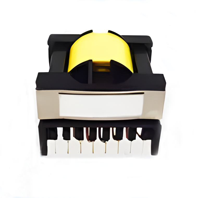 High Frequency Transformers
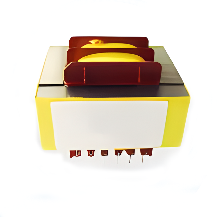 Low Frequency Transformers
 High Power Transformers
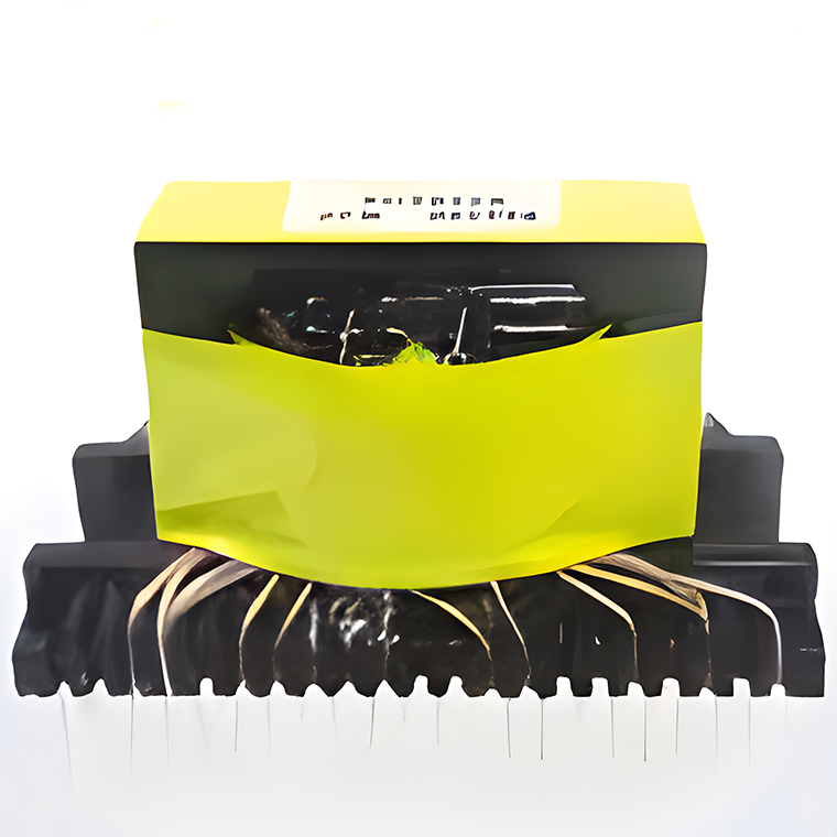 Conversion Transformers
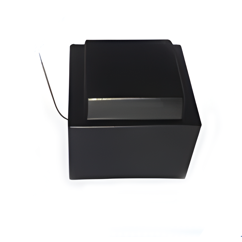 Sealed Transformers
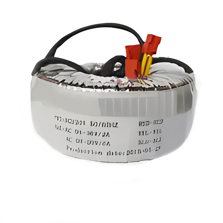 Ring Transformers
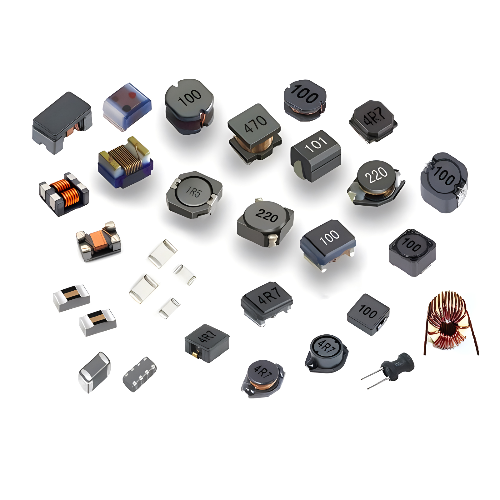 Inductors
 Wires,Cables Customized
 Network Cables
 Power Cords
 Antenna Cables
 Coaxial Cables
Zoning Design of Mixed-Signal PCBs
Abstract: The design of mixed-signal PCB (Printed Circuit Board) circuits is intricate, where the layout of components, routing, and the handling of power supplies and ground lines directly impact circuit performance and electromagnetic compatibility (EMC). This paper introduces a zoning design for ground and power supplies that can optimize the performance of mixed-signal circuits.
How can we reduce the mutual interference between digital and analog signals? Prior to design, it is crucial to understand two fundamental principles of EMC: the first principle is to minimize the area of current loops as much as possible; the second principle is to employ a single reference plane for the system. Conversely, if the system has two reference planes, it may form a dipole antenna (note: the radiation of a small dipole antenna is proportional to the length of the wires, the magnitude of the current flowing through them, and the frequency). Additionally, if signals cannot return through the smallest possible loops, a large loop antenna may be formed (note: the radiation of a small loop antenna is proportional to the loop area, the magnitude of the current flowing through the loop, and the square of the frequency). Both scenarios should be avoided as much as possible in design.
Some suggest segregating digital and analog grounds on mixed-signal boards to achieve isolation between them. While this approach is feasible, it poses numerous potential issues, particularly in complex, large-scale systems. The most critical issue is the inability to route wires across the split gaps, as doing so can dramatically increase electromagnetic radiation and signal crosstalk. The most common problem encountered in PCB design is EMI issues arising from signal lines crossing over split grounds or power supplies.


As shown in Figure 1, we adopt the aforementioned segmentation method, and when the signal line spans the gap between two grounds, what is the return path for the signal current? Assuming the two segmented grounds are connected somewhere (usually at a single point), in this case, the ground current will form a large loop. High-frequency currents flowing through this large loop generate radiation and high ground inductance. If low-level analog currents flow through this large loop, they are susceptible to external signal interference. The worst scenario is when the segmented grounds are connected at the power supply, forming an extremely large current loop. Additionally, connecting analog and digital grounds through a long wire creates a dipole antenna.
Understanding the path and manner of current returning to ground is crucial for optimizing mixed-signal PCB design. Many design engineers solely consider where the signal current flows, neglecting the specific current path. If ground plane segmentation is necessary, and routing must traverse the gap between segments, first establish a single-point connection between the segmented grounds, forming a bridge between them, and then route through this bridge. This ensures a direct current return path beneath each signal line, minimizing the loop area.
Optical isolators or transformers can also be employed to enable signals to cross segmented gaps. In the former case, optical signals traverse the gap; in the latter, magnetic fields do. Another viable option is using differential signals, where the signal flows into one line and returns through another, eliminating the need for a ground as a return path.
To delve into the interference of digital signals on analog signals, it's essential to understand the nature of high-frequency currents. High-frequency currents always choose the path of least impedance (lowest inductance), directly below the signal, hence return currents flow through adjacent circuit layers, be they power or ground planes.
In practice, it's common to use a unified ground and partition the PCB into analog and digital sections. Analog signals are routed within the analog area on all PCB layers, while digital signals are routed within the digital area. This prevents digital return currents from flowing into the analog ground.
Interference from digital signals to analog signals arises only when digital signals are routed over the analog section or vice versa. The root cause is not ground segmentation but improper routing of digital signals.
Adopting a unified ground in PCB design, partitioning digital and analog circuits, and appropriate signal routing often resolve complex layout and routing challenges without introducing potential issues from ground segmentation. In this case, component placement and partitioning become pivotal to design quality. With proper layout and routing, digital ground currents are confined to the digital section, avoiding interference with analog signals. Such routing requires meticulous inspection and verification to ensure 100% compliance with routing rules. Otherwise, a single misrouted signal line can ruin an otherwise excellent PCB.
When connecting the analog and digital ground pins of an A/D converter, most manufacturers recommend connecting the AGND and DGND pins with the shortest leads to a single low-impedance ground (note: most A/D converter chips do not internally connect analog and digital grounds, necessitating external pin connections). Any external impedance connected to DGND can couple more digital noise into the IC's internal analog circuitry through parasitic capacitance. Following this recommendation, both AGND and DGND pins of the A/D converter should be connected to the analog ground, but this raises questions about where to ground the decoupling capacitors for digital signals—to analog or digital ground.
If the system has only one A/D converter, the solution is straightforward. As shown in Figure 3, split the ground and connect the analog and digital ground sections beneath the A/D converter. When doing so, ensure the bridge connecting the two grounds is as wide as the IC, and no signal lines cross the gap.

If there are many A/D converters in the system, such as 10 A/D converters, how to connect them? If the analog ground and digital ground are connected together under each A/D converter, it will result in multiple points of connection, and the isolation between the analog ground and digital ground will be meaningless. If not connected in this way, it will violate the manufacturer's requirements.
The best way is to use a unified ground at the beginning. As shown in Figure 4, the unified ground is divided into an analog part and a digital part. This layout and wiring not only meets the requirements of IC device manufacturers for low-impedance connections between analog and digital ground pins, but also does not create loop antennas or dipole antennas that can cause EMC problems.

If you have doubts about using a unified approach for mixed-signal PCB design, you can use the ground layer segmentation method to lay out and route the entire circuit board. During design, pay attention to making it easier for the circuit board to be connected together using jumpers with a spacing of less than 1/2 inch or 0 ohm resistors during later experiments. Pay attention to partitioning and routing, ensuring that no digital signal lines are located above the analog part on all layers, and no analog signal lines are located above the digital part. Moreover, no signal line can cross the ground gap or divide the gap between power supplies. To test the function and EMC performance of the circuit board, connect the two grounds together using a 0 ohm resistor or jumper, and retest the function and EMC performance of the circuit board. Comparing the test results, it will be found that in almost all cases, the unified approach is superior to the divided approach in terms of function and EMC performance.
#Is the method of dividing the land still useful?
This method can be used in the following three situations: some medical equipment requires low leakage current between the circuits and systems connected to the patient; the output of some industrial process control equipment may be connected to electromechanical devices with high noise and high power; another situation is when the layout of the PCB is subject to specific restrictions.
There are usually separate digital and analog power supplies on mixed-signal PCB boards, and it can and should be possible to use a split power plane. However, signal lines that are immediately adjacent to the power plane cannot cross the gap between power supplies, and all signal lines that cross this gap must be located on the circuit layer immediately adjacent to the large ground plane. In some cases, designing the analog power supply with PCB connecting lines rather than a single plane can avoid the problem of splitting the power plane.
Mixed-signal PCB design is a complex process, and the following points should be noted during the design process:
- Divide the PCB into separate analog and digital sections.
- Proper layout of components.
- A/D converters are placed across the partition.
- Do not divide the ground. Lay the analog and digital parts of the circuit board uniformly under the ground.
- In all layers of the circuit board, digital signals can only be routed in the digital part of the board.
- In all layers of the circuit board, analog signals can only be routed in the analog part of the board.
- Implement the division of analog and digital power sources.
- Wiring cannot cross the gap between the divided power supply surfaces.
- The signal line that must cross the gap between the split power supplies should be located on the wiring layer immediately adjacent to the large area ground.
- Analyze the actual path and mode of the current flowing back to the ground.
- Adopt the correct wiring rules.